- 您现在的位置:买卖IC网 > PDF目录224620 > OP-37GP (TEXAS INSTRUMENTS INC) OP-AMP, 220 uV OFFSET-MAX, 63 MHz BAND WIDTH, PDIP8 PDF资料下载
参数资料
| 型号: | OP-37GP |
| 厂商: | TEXAS INSTRUMENTS INC |
| 元件分类: | 运算放大器 |
| 英文描述: | OP-AMP, 220 uV OFFSET-MAX, 63 MHz BAND WIDTH, PDIP8 |
| 封装: | PLASTIC, DIP-8 |
| 文件页数: | 8/24页 |
| 文件大小: | 391K |
| 代理商: | OP-37GP |
OP27A, OP27C, OP27E, OP27G
OP37A, OP37C, OP37E, OP37G
LOW-NOISE HIGH-SPEED PRECISION OPERATIONAL-AMPLIFIER
SLOS100C – FEBRUARY 1989 – REVISED SEPTEMBER 2000
16
POST OFFICE BOX 655303
DALLAS, TEXAS 75265
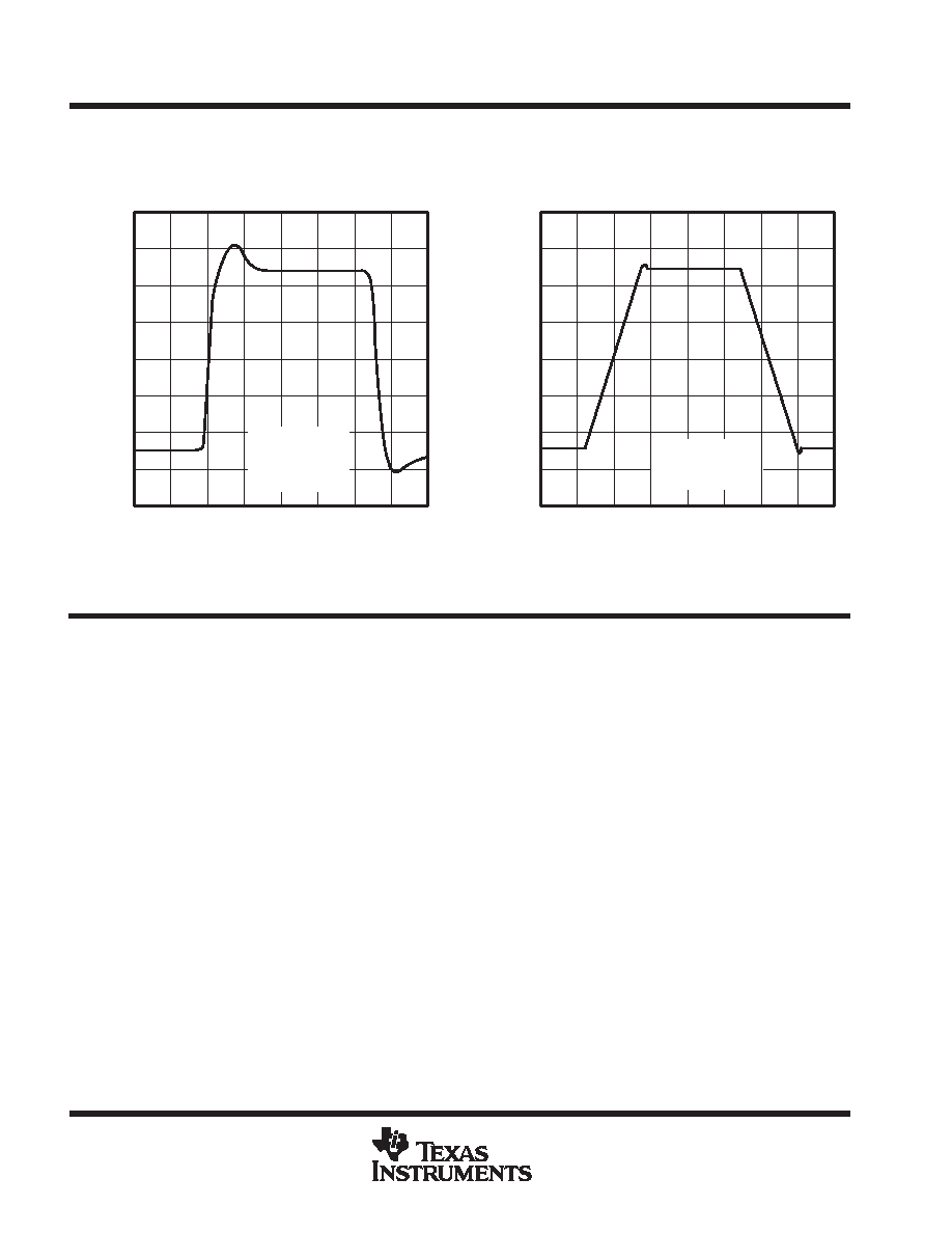
TYPICAL CHARACTERISTICS
V
OP37
VOLTAGE-FOLLOWER
SMALL-SIGNAL PULSE RESPONSE
80
60
40
20
0
– 20
– 40
– 60
– 80
O
–
Output
V
oltage
–
mV
t – Time –
s
0
0.2
0.4
0.6
0.8
1
1.2
VCC
± = ±15 V
AV = 5
CL = 15 pF
TA = 25°C
V
O
–
Output
V
oltage
–
V
OP37
VOLTAGE-FOLLOWER
LARGE-SIGNAL PULSE RESPONSE
8
6
4
0
– 2
– 4
– 6
– 8
2
t – Time –
s
012
345
6
VCC
± = ±15 V
AV = 5
TA = 25°C
Figure 32
Figure 33
APPLICATION INFORMATION
general
The OP27 and OP37 series devices can be inserted directly onto OP07, OP05,
A725, and SE5534 sockets
with or without removing external compensation or nulling components. In addition, the OP27 and OP37 can
be fitted to
A741 sockets by removing or modifying external nulling components.
noise testing
Figure 34 shows a test circuit for 0.1-Hz to 10-Hz peak-to-peak noise measurement of the OP27 and OP37.
The frequency response of this noise tester indicates that the 0.1-Hz corner is defined by only one zero.
Because the time limit acts as an additional zero to eliminate noise contributions from the frequency band below
0.1 Hz, the test time to measure 0.1-Hz to 10-Hz noise should not exceed 10 seconds.
Measuring the typical 80-nV peak-to-peak noise performance of the OP27 and OP37 requires the following
special test precautions:
1.
The device should be warmed up for at least five minutes. As the operational amplifier warms up, the
offset voltage typically changes 4
V due to the chip temperature increasing from 10°C to 20°C starting
from the moment the power supplies are turned on. In the 10-s measurement interval, these
temperature-induced effects can easily exceed tens of nanovolts.
2.
For similar reasons, the device should be well shielded from air currents to eliminate the possibility of
thermoelectric effects in excess of a few nanovolts, which would invalidate the measurements.
3.
Sudden motion in the vicinity of the device should be avoided, as it produces a feedthrough effect that
increases observed noise.
相关PDF资料 |
PDF描述 |
|---|---|
| OP-47GT | OP-AMP, 220 uV OFFSET-MAX, 70 MHz BAND WIDTH, MBCY8 |
| OP-47CD/883B | OP-AMP, 300 uV OFFSET-MAX, 70 MHz BAND WIDTH, CDIP8 |
| OP-47CT/883B | OP-AMP, 300 uV OFFSET-MAX, 70 MHz BAND WIDTH, MBCY8 |
| OP-47CD | OP-AMP, 300 uV OFFSET-MAX, 70 MHz BAND WIDTH, CDIP8 |
| OP-47CT | OP-AMP, 300 uV OFFSET-MAX, 70 MHz BAND WIDTH, MBCY8 |
相关代理商/技术参数 |
参数描述 |
|---|---|
| OP37GP+ | 功能描述:运算放大器 - 运放 RoHS:否 制造商:STMicroelectronics 通道数量:4 共模抑制比(最小值):63 dB 输入补偿电压:1 mV 输入偏流(最大值):10 pA 工作电源电压:2.7 V to 5.5 V 安装风格:SMD/SMT 封装 / 箱体:QFN-16 转换速度:0.89 V/us 关闭:No 输出电流:55 mA 最大工作温度:+ 125 C 封装:Reel |
| OP37GPZ | 功能描述:IC OPAMP GP 63MHZ LN PREC 8DIP RoHS:是 类别:集成电路 (IC) >> Linear - Amplifiers - Instrumentation 系列:- 产品培训模块:Differential Circuit Design Techniques for Communication Applications 标准包装:1 系列:- 放大器类型:RF/IF 差分 电路数:1 输出类型:差分 转换速率:9800 V/µs 增益带宽积:- -3db带宽:2.9GHz 电流 - 输入偏压:3µA 电压 - 输入偏移:- 电流 - 电源:40mA 电流 - 输出 / 通道:- 电压 - 电源,单路/双路(±):3 V ~ 3.6 V 工作温度:-40°C ~ 85°C 安装类型:表面贴装 封装/外壳:16-VQFN 裸露焊盘,CSP 供应商设备封装:16-LFCSP-VQ 包装:剪切带 (CT) 产品目录页面:551 (CN2011-ZH PDF) 其它名称:ADL5561ACPZ-R7CT |
| OP37GS | 功能描述:运算放大器 - 运放 RoHS:否 制造商:STMicroelectronics 通道数量:4 共模抑制比(最小值):63 dB 输入补偿电压:1 mV 输入偏流(最大值):10 pA 工作电源电压:2.7 V to 5.5 V 安装风格:SMD/SMT 封装 / 箱体:QFN-16 转换速度:0.89 V/us 关闭:No 输出电流:55 mA 最大工作温度:+ 125 C 封装:Reel |
| OP-37GS | 制造商:AD 制造商全称:Analog Devices 功能描述:LOW NOISE, PRECISION, HIGH SPEED OPERATIONAL AMPLIFIER(AVCL>=5) |
| OP37GS+ | 功能描述:运算放大器 - 运放 RoHS:否 制造商:STMicroelectronics 通道数量:4 共模抑制比(最小值):63 dB 输入补偿电压:1 mV 输入偏流(最大值):10 pA 工作电源电压:2.7 V to 5.5 V 安装风格:SMD/SMT 封装 / 箱体:QFN-16 转换速度:0.89 V/us 关闭:No 输出电流:55 mA 最大工作温度:+ 125 C 封装:Reel |
发布紧急采购,3分钟左右您将得到回复。