参数资料
| 型号: | OP249AZ |
| 厂商: | Analog Devices Inc |
| 文件页数: | 6/20页 |
| 文件大小: | 0K |
| 描述: | IC OPAMP JFET 4.7MHZ DUAL 8CDIP |
| 标准包装: | 1 |
| 放大器类型: | J-FET |
| 电路数: | 2 |
| 转换速率: | 22 V/µs |
| 增益带宽积: | 4.7MHz |
| 电流 - 输入偏压: | 30pA |
| 电压 - 输入偏移: | 200µV |
| 电流 - 电源: | 5.6mA |
| 电流 - 输出 / 通道: | 36mA |
| 电压 - 电源,单路/双路(±): | ±4.5 V ~ 18 V |
| 工作温度: | -55°C ~ 125°C |
| 安装类型: | 通孔 |
| 封装/外壳: | 8-CDIP(0.300",7.62mm) |
| 供应商设备封装: | 8-CERDIP |
| 包装: | 管件 |
OP249
Data Sheet
Rev. H | Page 14 of 20
10
0%
100
90
50mV
1s
00296-
042
Figure 42. Small-Signal Transient Response,
AV = 1, ZL = 2 k||100 pF, No Compensation, VS = ±15 V
As with most JFET input amplifiers, the output of the OP249
can undergo phase inversion if either input exceeds the specified
input voltage range. Phase inversion does not damage the
amplifier, nor does it cause an internal latch-up condition.
Supply decoupling should be used to overcome inductance and
resistance associated with supply lines to the amplifier. A 0.1 F
and a 10 F capacitor should be placed between each supply pin
and ground.
OPEN-LOOP GAIN LINEARITY
The OP249 has both an extremely high open-loop gain of
1 kV/mV minimum and constant gain linearity, which enhances its
dc precision and provides superb accuracy in high closed-loop
gain applications. Figure 43 illustrates the typical open-loop
gain linearity—high gain accuracy is assured, even when
driving a 600 Ω load.
OFFSET VOLTAGE ADJUSTMENT
The inherent low offset voltage of the OP249 makes offset
adjustments unnecessary in most applications. However, where
a lower offset error is required, balancing can be performed
with simple external circuitry, as shown in Figure 44 and Figure 45.
HORIZONTAL 5V/DIV
OUTPUT CHARGE
VERTICAL 50V/DIV
INPUT VARIATION
00296-
043
Figure 43. Open-Loop Gain Linearity; Variation in Open-Loop Gain Results in
Errors in High Closed-Loop Gain Circuits; RL = 600 , VS = ±15 V
+V
R3
R4
R2
R1
VOS ADJUST RANGE = ±V
VOUT
VIN
–V
1/2
OP249
R2
31
R5
50k
R1
200k
00296-
044
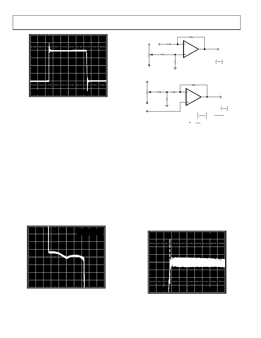
Figure 44. Offset Adjustment for Inverting Amplifier Configuration
+V
R5
VOS ADJUST RANGE = ±V
R2
R1
1 +
R5
R4
IF R2 << R4
R5
R4 + R2
R4
VOUT
–V
VIN
R3
50k
R2
33
R1
200k
1/2
OP249
GAIN =
= 1 +
VOUT
VIN
=
00296-
045
Figure 45. Offset Adjustment for Noninverting Amplifier Configuration
In Figure 44, the offset adjustment is made by supplying a small
voltage at the noninverting input of the amplifier. Resistors R1
and R2 attenuate the potentiometer voltage, providing a ±2.5 mV
(with VS = ±15 V) adjustment range, referred to the input.
Figure 45 shows the offset adjustment for the noninverting
amplifier configuration, also providing a ±2.5 mV adjustment
range. As shown in the equations in Figure 45, if R4 is not much
greater than R2, a resulting closed-loop gain error must be
accounted for.
SETTLING TIME
The settling time is the time between when the input signal begins
to change and when the output permanently enters a prescribed
error band. The error bands on the output are 5 mV and 0.5 mV,
respectively, for 0.1% and 0.01% accuracy.
Figure 46 shows the settling time of the OP249, which is typically
870 ns. Moreover, problems in settling response, such as thermal
tails and long-term ringing, are nonexistent.
10
0%
100
90
500ns
10mV
870ns
00296-
046
Figure 46. Settling Characteristics of the OP249 to 0.01%
相关PDF资料 |
PDF描述 |
|---|---|
| OP262GSZ-REEL7 | IC OPAMP GP R-R 15MHZ DUAL 8SOIC |
| OP270GS | IC OPAMP GP 5MHZ DUAL LN 16SOIC |
| OP279GS | IC OPAMP GP R-R 5MHZ DUAL 8SOIC |
| OP27GS | IC OPAMP GP 8MHZ LN PREC 8SOIC |
| OP282GS | IC OPAMP JFET 4MHZ DUAL LP 8SOIC |
相关代理商/技术参数 |
参数描述 |
|---|---|
| OP249AZ/883 | 制造商:未知厂家 制造商全称:未知厂家 功能描述:OP-AMP|DUAL|BIPOLAR/JFET|DIP|8PIN|CERAMIC |
| OP249AZMDA | 制造商:Analog Devices 功能描述: |
| OP249EJ | 制造商:AD 制造商全称:Analog Devices 功能描述:Dual, Precision JFET High Speed Operational Amplifier |
| OP249EZ | 制造商:Rochester Electronics LLC 功能描述:- Bulk |
| OP249FJ | 制造商:Rochester Electronics LLC 功能描述:- Bulk |
发布紧急采购,3分钟左右您将得到回复。