参数资料
| 型号: | OP249GP |
| 厂商: | Analog Devices Inc |
| 文件页数: | 8/20页 |
| 文件大小: | 0K |
| 描述: | IC OPAMP JFET 4.7MHZ DUAL 8DIP |
| 标准包装: | 50 |
| 放大器类型: | J-FET |
| 电路数: | 2 |
| 转换速率: | 22 V/µs |
| 增益带宽积: | 4.7MHz |
| 电流 - 输入偏压: | 30pA |
| 电压 - 输入偏移: | 200µV |
| 电流 - 电源: | 5.6mA |
| 电流 - 输出 / 通道: | 36mA |
| 电压 - 电源,单路/双路(±): | ±4.5 V ~ 18 V |
| 工作温度: | -40°C ~ 85°C |
| 安装类型: | 通孔 |
| 封装/外壳: | 8-DIP(0.300",7.62mm) |
| 供应商设备封装: | 8-PDIP |
| 包装: | 管件 |
OP249
Data Sheet
Rev. H | Page 16 of 20
10
0%
100
90
500mV
1s
4s
10
0%
100
90
500mV
1s
4s
A
C = 5pF
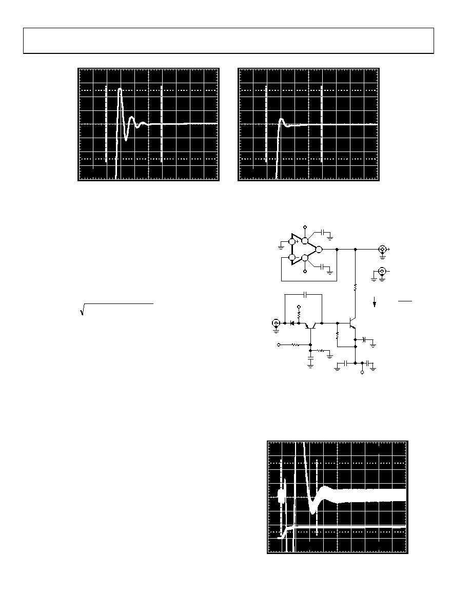
RESPONSE IS GROSSLY UNDERDAMPED,
AND EXHIBITS RINGING
B
C = 15pF
FAST RISE TIME CHARACTERISTICS, BUT AT EXPENSE
OF SLIGHT PEAKING IN RESPONSE
00296-
049
Figure 49. Effect of Altering Compensation from Circuit in Figure 47—PM7545 CMOS DAC with 1/2 OP249, Unipolar Operation;
Critically Damped Response Is Obtained with C ≈ 33 pF
Figure 49 illustrates the effect of altering the compensation on
the output response of the circuit in Figure 47. Compensation is
required to address the combined effect of the output capacitance
of the DAC, the input capacitance of the op amp, and any stray
capacitance. Slight adjustments to the compensation capacitor may
be required to optimize settling response for any given application.
The settling time of the combination of the current output DAC
and the op amp can be approximated by
(
) (
)2
2
AMP
t
DAC
t
TOTAL
t
S
+
=
The actual overall settling time is affected by the noise gain of
the amplifier, the applied compensation, and the equivalent
input capacitance at the input of the amplifier.
DISCUSSION ON DRIVING ADCs
Settling characteristics of op amps also include the ability of the
amplifier to recover, that is, settle, from a transient current output
load condition. An example of this includes an op amp driving
the input from a SAR-type ADC. Although the comparison
point of the converter is usually diode clamped, the input swing
of plus-and-minus a diode drop still gives rise to a significant
modulation of input current. If the closed-loop output impedance
is low enough and bandwidth of the amplifier is sufficiently
large, the output settles before the converter makes a comparison
decision, which prevents linearity errors or missing codes.
Figure 50 shows a settling measurement circuit for evaluating
recovery from an output current transient. An output disturbing
current generator provides the transient change in output load
current of 1 mA.
+15V
1.5k
1N4148
220
1.8k
2N3904
1k
*
TTL INPUT
+15V
2N2907
7A13 PLUG-IN
300pF
1/2
OP249
+
1k
|VREF|
ΔIOUT =
–15V
0.1F
10F
VREF
0.01F
1k
0.47F
3
2
8
1
4
*DECOUPLE CLOSE TOGETHER ON GROUND
PLANE WITH SHORT LEAD LENGTHS.
00296-
050
Figure 50. Transient Output Impedance Test Fixture
As seen in Figure 51, the OP249 has an extremely fast recovery
of 247 ns (to 0.01%) for a 1 mA load transient. The performance
makes it an ideal amplifier for data acquisition systems.
10
0%
100
90
100ns
2V
2mV
247.4ns
00296-
051
Figure 51. Transient Recovery Time of the OP249 from
a 1 mA Load Transient to 0.01%
相关PDF资料 |
PDF描述 |
|---|---|
| D-150-0237 | CONN SPLICE BUTT 16-18AWG BLUE |
| 77311-101-07LF | HDR STR SR. 100 DP |
| TSW-134-06-G-D | CONN HEADER 68POS .100" DL GOLD |
| 77315-113-04LF | BERGSTIK |
| TSW-134-05-G-D | CONN HEADER 68POS .100" DL GOLD |
相关代理商/技术参数 |
参数描述 |
|---|---|
| OP249GPZ | 功能描述:IC OPAMP JFET 4.7MHZ DUAL 8DIP RoHS:是 类别:集成电路 (IC) >> Linear - Amplifiers - Instrumentation 系列:- 标准包装:2,500 系列:- 放大器类型:通用 电路数:4 输出类型:- 转换速率:0.6 V/µs 增益带宽积:1MHz -3db带宽:- 电流 - 输入偏压:45nA 电压 - 输入偏移:2000µV 电流 - 电源:1.4mA 电流 - 输出 / 通道:40mA 电压 - 电源,单路/双路(±):3 V ~ 32 V,±1.5 V ~ 16 V 工作温度:0°C ~ 70°C 安装类型:表面贴装 封装/外壳:14-TSSOP(0.173",4.40mm 宽) 供应商设备封装:14-TSSOP 包装:带卷 (TR) 其它名称:LM324ADTBR2G-NDLM324ADTBR2GOSTR |
| OP249GS | 功能描述:IC OPAMP JFET 4.7MHZ DUAL 8SOIC RoHS:否 类别:集成电路 (IC) >> Linear - Amplifiers - Instrumentation 系列:- 标准包装:73 系列:Over-The-Top® 放大器类型:通用 电路数:4 输出类型:满摆幅 转换速率:0.07 V/µs 增益带宽积:200kHz -3db带宽:- 电流 - 输入偏压:1nA 电压 - 输入偏移:285µV 电流 - 电源:50µA 电流 - 输出 / 通道:25mA 电压 - 电源,单路/双路(±):2 V ~ 44 V,±1 V ~ 22 V 工作温度:-40°C ~ 85°C 安装类型:表面贴装 封装/外壳:16-WFDFN 裸露焊盘 供应商设备封装:16-DFN-EP(5x3) 包装:管件 |
| OP249GS-REEL | 功能描述:IC OPAMP JFET 4.7MHZ DUAL 8SOIC RoHS:否 类别:集成电路 (IC) >> Linear - Amplifiers - Instrumentation 系列:- 标准包装:50 系列:LinCMOS™ 放大器类型:通用 电路数:4 输出类型:- 转换速率:0.05 V/µs 增益带宽积:110kHz -3db带宽:- 电流 - 输入偏压:0.7pA 电压 - 输入偏移:210µV 电流 - 电源:57µA 电流 - 输出 / 通道:30mA 电压 - 电源,单路/双路(±):3 V ~ 16 V,±1.5 V ~ 8 V 工作温度:-40°C ~ 85°C 安装类型:表面贴装 封装/外壳:14-SOIC(0.154",3.90mm 宽) 供应商设备封装:14-SOIC 包装:管件 产品目录页面:865 (CN2011-ZH PDF) 其它名称:296-1834296-1834-5 |
| OP249GS-REEL7 | 功能描述:IC OPAMP JFET 4.7MHZ DUAL 8SOIC RoHS:否 类别:集成电路 (IC) >> Linear - Amplifiers - Instrumentation 系列:- 标准包装:50 系列:LinCMOS™ 放大器类型:通用 电路数:4 输出类型:- 转换速率:0.05 V/µs 增益带宽积:110kHz -3db带宽:- 电流 - 输入偏压:0.7pA 电压 - 输入偏移:210µV 电流 - 电源:57µA 电流 - 输出 / 通道:30mA 电压 - 电源,单路/双路(±):3 V ~ 16 V,±1.5 V ~ 8 V 工作温度:-40°C ~ 85°C 安装类型:表面贴装 封装/外壳:14-SOIC(0.154",3.90mm 宽) 供应商设备封装:14-SOIC 包装:管件 产品目录页面:865 (CN2011-ZH PDF) 其它名称:296-1834296-1834-5 |
| OP249GSZ | 功能描述:IC OPAMP JFET 4.7MHZ DUAL 8SOIC RoHS:是 类别:集成电路 (IC) >> Linear - Amplifiers - Instrumentation 系列:- 标准包装:2,500 系列:- 放大器类型:通用 电路数:4 输出类型:- 转换速率:0.6 V/µs 增益带宽积:1MHz -3db带宽:- 电流 - 输入偏压:45nA 电压 - 输入偏移:2000µV 电流 - 电源:1.4mA 电流 - 输出 / 通道:40mA 电压 - 电源,单路/双路(±):3 V ~ 32 V,±1.5 V ~ 16 V 工作温度:0°C ~ 70°C 安装类型:表面贴装 封装/外壳:14-TSSOP(0.173",4.40mm 宽) 供应商设备封装:14-TSSOP 包装:带卷 (TR) 其它名称:LM324ADTBR2G-NDLM324ADTBR2GOSTR |
发布紧急采购,3分钟左右您将得到回复。