参数资料
| 型号: | OP262GSZ |
| 厂商: | Analog Devices Inc |
| 文件页数: | 5/20页 |
| 文件大小: | 0K |
| 描述: | IC OPAMP GP R-R 15MHZ DUAL 8SOIC |
| 标准包装: | 98 |
| 放大器类型: | 通用 |
| 电路数: | 2 |
| 输出类型: | 满摆幅 |
| 转换速率: | 13 V/µs |
| 增益带宽积: | 15MHz |
| 电流 - 输入偏压: | 260nA |
| 电压 - 输入偏移: | 25µV |
| 电流 - 电源: | 550µA |
| 电流 - 输出 / 通道: | 30mA |
| 电压 - 电源,单路/双路(±): | 2.7 V ~ 12 V,±1.35 V ~ 6 V |
| 工作温度: | -40°C ~ 125°C |
| 安装类型: | 表面贴装 |
| 封装/外壳: | 8-SOIC(0.154",3.90mm 宽) |
| 供应商设备封装: | 8-SO |
| 包装: | 管件 |
| 产品目录页面: | 774 (CN2011-ZH PDF) |
Data Sheet
OP162/OP262/OP462
Rev. H | Page 13 of 20
and VIN swings up to 5 V, the output current will not exceed
30 mA. For single 5 V supply applications, resistors less than
169 are not recommended.
Figure 32. Output Short-Circuit Protection
INPUT OVERVOLTAGE PROTECTION
The input voltage should be limited to ±6 V, or damage to the
device can occur. Electrostatic protection diodes placed in the
input stage of the device help protect the amplifier from static
discharge. Diodes are connected between each input as well as
from each input to both supply pins as shown in the simplified
equivalent circuit in Figure 30. If an input voltage exceeds either
supply voltage by more than 0.6 V, or if the differential input
voltage is greater than 0.6 V, these diodes energize causing
overvoltage damage.
The input current should be limited to less than 5 mA to
prevent degradation or destruction of the device by placing an
external resistor in series with the input at risk of being overdriven.
The size of the resistor can be calculated by dividing the maxi-
mum input voltage by 5 mA. For example, if the differential
input voltage could reach 5 V, the external resistor should be
5 V/5 mA = 1 k. In practice, this resistor should be placed in
series with both inputs to balance any offset voltages created by
the input bias current.
OUTPUT PHASE REVERSAL
The OP162/OP262/OP462 are immune to phase reversal as
long as the input voltage is limited to ±6 V. Figure 27 shows the
output of a device with the input voltage driven beyond the
supply voltages. Although the device’s output does not change
phase, large currents due to input overvoltage could result,
damaging the device. In applications where the possibility of an
input voltage exceeding the supply voltage exists, overvoltage
protection should be used, as described in the previous section.
POWER DISSIPATION
The maximum power that can be safely dissipated by the
OP162/OP262/OP462 is limited by the associated rise in
junction temperature. The maximum safe junction temperature
is 150°C; device performance suffers when this limit is
exceeded. If this maximum is only momentarily exceeded,
proper circuit operation will be restored as soon as the die
temperature is reduced. Leaving the device in an “overheated”
condition for an extended period can result in permanent
damage to the device.
To calculate the internal junction temperature of the OPx62, use
the formula
TJ = PDISS × θJA + TA
where:
TJ is the OPx62 junction temperature.
PDISS is the OPx62 power dissipation.
θJA is the OPx62 package thermal resistance, junction-to-
ambient temperature.
TA is the ambient temperature of the circuit.
The power dissipated by the device can be calculated as
PDISS = ILOAD × (VS – VOUT)
where:
ILOAD is the OPx62 output load current.
VS is the OPx62 supply voltage.
VOUT is the OPx62 output voltage.
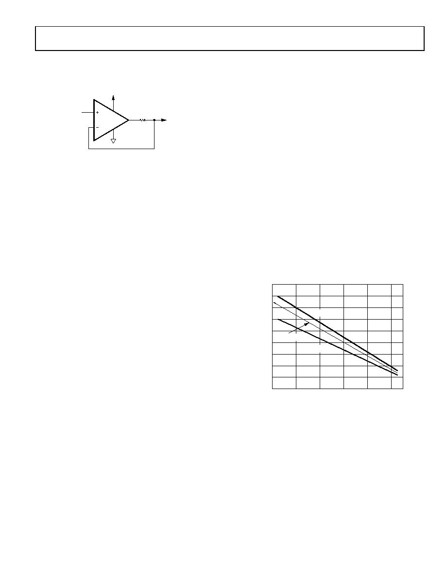
Figure 33 and Figure 34 provide a convenient way to determine
if the device is being overheated. The maximum safe power
dissipation can be found graphically, based on the package type
and the ambient temperature around the package. By using the
previous equation, it is a simple matter to see if PDISS exceeds the
device’s power derating curve. To ensure proper operation, it is
important to observe the recommended derating curves shown
Figure 33. Maximum Power Dissipation vs. Temperature for
8-Lead Package Types
OPx62
VIN
VOUT
169
5V
00288-035
AMBIENT TEMPERATURE (
°C)
MAXIMUM
POWER
DISSIPATION
(Watts)
0.9
0.7
0.8
0.5
0.6
0.1
0.2
0.3
0.4
0
20
40
60
100
80
120
00288-036
8-LEAD SOIC
8-LEAD MSOP
8-LEAD TSSOP
相关PDF资料 |
PDF描述 |
|---|---|
| PEC05DBBN | CONN HEADER .100 DUAL R/A 10POS |
| PEC36SAFN | CONN HEADER .100 SINGL STR 36POS |
| AD8475ARMZ | IC OP AMP R-R FUNNEL 10 MSOP |
| PEC16DAAN | CONN HEADER .100 DUAL STR 32POS |
| PEC15SACN | CONN HEADER .100 SINGL STR 15POS |
相关代理商/技术参数 |
参数描述 |
|---|---|
| OP262GSZ-REEL | 功能描述:IC OPAMP GP R-R 15MHZ DUAL 8SOIC RoHS:是 类别:集成电路 (IC) >> Linear - Amplifiers - Instrumentation 系列:- 标准包装:50 系列:LinCMOS™ 放大器类型:通用 电路数:4 输出类型:- 转换速率:0.05 V/µs 增益带宽积:110kHz -3db带宽:- 电流 - 输入偏压:0.7pA 电压 - 输入偏移:210µV 电流 - 电源:57µA 电流 - 输出 / 通道:30mA 电压 - 电源,单路/双路(±):3 V ~ 16 V,±1.5 V ~ 8 V 工作温度:-40°C ~ 85°C 安装类型:表面贴装 封装/外壳:14-SOIC(0.154",3.90mm 宽) 供应商设备封装:14-SOIC 包装:管件 产品目录页面:865 (CN2011-ZH PDF) 其它名称:296-1834296-1834-5 |
| OP262GSZ-REEL7 | 功能描述:IC OPAMP GP R-R 15MHZ DUAL 8SOIC RoHS:是 类别:集成电路 (IC) >> Linear - Amplifiers - Instrumentation 系列:- 标准包装:1 系列:- 放大器类型:通用 电路数:4 输出类型:满摆幅 转换速率:0.6 V/µs 增益带宽积:1MHz -3db带宽:- 电流 - 输入偏压:2pA 电压 - 输入偏移:1000µV 电流 - 电源:85µA 电流 - 输出 / 通道:20mA 电压 - 电源,单路/双路(±):1.8 V ~ 6 V 工作温度:-40°C ~ 125°C 安装类型:表面贴装 封装/外壳:14-SOIC(0.154",3.90mm 宽) 供应商设备封装:14-SOICN 包装:剪切带 (CT) 产品目录页面:680 (CN2011-ZH PDF) 其它名称:MCP6L04T-E/SLCT |
| OP262HRU | 制造商:Analog Devices 功能描述:OP Amp Dual GP R-R O/P |
| OP262HRU-REEL | 功能描述:IC OPAMP GP R-R 15MHZ LN 8TSSOP RoHS:否 类别:集成电路 (IC) >> Linear - Amplifiers - Instrumentation 系列:- 标准包装:1 系列:- 放大器类型:通用 电路数:4 输出类型:满摆幅 转换速率:0.028 V/µs 增益带宽积:105kHz -3db带宽:- 电流 - 输入偏压:3nA 电压 - 输入偏移:100µV 电流 - 电源:3.3µA 电流 - 输出 / 通道:12mA 电压 - 电源,单路/双路(±):2.7 V ~ 12 V,±1.35 V ~ 6 V 工作温度:-40°C ~ 85°C 安装类型:表面贴装 封装/外壳:14-TSSOP(0.173",4.40mm 宽) 供应商设备封装:14-TSSOP 包装:剪切带 (CT) 其它名称:OP481GRUZ-REELCT |
| OP262HRUZ | 功能描述:IC OPAMP GP R-R 15MHZ LN 8TSSOP RoHS:是 类别:集成电路 (IC) >> Linear - Amplifiers - Instrumentation 系列:- 标准包装:2,500 系列:- 放大器类型:通用 电路数:4 输出类型:- 转换速率:0.6 V/µs 增益带宽积:1MHz -3db带宽:- 电流 - 输入偏压:45nA 电压 - 输入偏移:2000µV 电流 - 电源:1.4mA 电流 - 输出 / 通道:40mA 电压 - 电源,单路/双路(±):3 V ~ 32 V,±1.5 V ~ 16 V 工作温度:0°C ~ 70°C 安装类型:表面贴装 封装/外壳:14-TSSOP(0.173",4.40mm 宽) 供应商设备封装:14-TSSOP 包装:带卷 (TR) 其它名称:LM324ADTBR2G-NDLM324ADTBR2GOSTR |
发布紧急采购,3分钟左右您将得到回复。