- 您现在的位置:买卖IC网 > PDF目录296742 > OP262HRUZ-REEL (ANALOG DEVICES INC) 15 MHz Rail-to-Rail Operational Amplifier, Dual; Package: TSSOP; No of Pins: 8; Temperature Range: Industrial PDF资料下载
参数资料
| 型号: | OP262HRUZ-REEL |
| 厂商: | ANALOG DEVICES INC |
| 元件分类: | 运算放大器 |
| 英文描述: | 15 MHz Rail-to-Rail Operational Amplifier, Dual; Package: TSSOP; No of Pins: 8; Temperature Range: Industrial |
| 中文描述: | DUAL OP-AMP, 1000 uV OFFSET-MAX, 15 MHz BAND WIDTH, PDSO8 |
| 封装: | LEAD FREE, MS-153AA, TSSOP-8 |
| 文件页数: | 5/20页 |
| 文件大小: | 949K |
| 代理商: | OP262HRUZ-REEL |
OP162/OP262/OP462
Rev. F | Page 13 of 20
and VIN swings up to 5 V, the output current will not exceed
30 mA. For single 5 V supply applications, resistors less than
169 are not recommended.
OPx62
VIN
VOUT
169
5V
00288-035
Figure 35. Output Short-Circuit Protection
INPUT OVERVOLTAGE PROTECTION
The input voltage should be limited to ±6 V, or damage to the
device can occur. Electrostatic protection diodes placed in the
input stage of the device help protect the amplifier from static
discharge. Diodes are connected between each input as well as
from each input to both supply pins as shown in the simplified
equivalent circuit in Figure 33. If an input voltage exceeds either
supply voltage by more than 0.6 V, or if the differential input
voltage is greater than 0.6 V, these diodes energize causing
overvoltage damage.
The input current should be limited to less than 5 mA to
prevent degradation or destruction of the device by placing an
external resistor in series with the input at risk of being overdriven.
The size of the resistor can be calculated by dividing the maxi-
mum input voltage by 5 mA. For example, if the differential
input voltage could reach 5 V, the external resistor should be
5 V/5 mA = 1 k. In practice, this resistor should be placed in
series with both inputs to balance any offset voltages created by
the input bias current.
OUTPUT PHASE REVERSAL
The OP162/OP262/OP462 are immune to phase reversal as
long as the input voltage is limited to ±6 V. Figure 30 shows the
output of a device with the input voltage driven beyond the
supply voltages. Although the device’s output does not change
phase, large currents due to input overvoltage could result,
damaging the device. In applications where the possibility of an
input voltage exceeding the supply voltage exists, overvoltage
protection should be used, as described in the previous section.
POWER DISSIPATION
The maximum power that can be safely dissipated by the
OP162/OP262/OP462 is limited by the associated rise in
junction temperature. The maximum safe junction temperature
is 150°C; device performance suffers when this limit is
exceeded. If this maximum is only momentarily exceeded,
proper circuit operation will be restored as soon as the die
temperature is reduced. Leaving the device in an “overheated”
condition for an extended period can result in permanent
damage to the device.
To calculate the internal junction temperature of the OPx62, use
the formula
TJ = PDISS × θJA + TA
where:
TJ is the OPx62 junction temperature.
PDISS is the OPx62 power dissipation.
θJA is the OPx62 package thermal resistance, junction-to-
ambient temperature.
TA is the ambient temperature of the circuit.
The power dissipated by the device can be calculated as
PDISS = ILOAD × (VS – VOUT)
where:
ILOAD is the OPx62 output load current.
VS is the OPx62 supply voltage.
VOUT is the OPx62 output voltage.
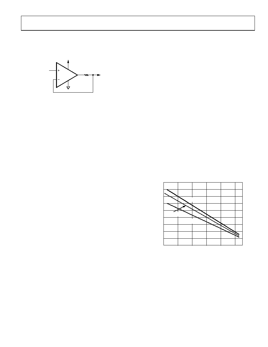
Figure 36 and Figure 37 provide a convenient way to determine
if the device is being overheated. The maximum safe power
dissipation can be found graphically, based on the package type
and the ambient temperature around the package. By using the
previous equation, it is a simple matter to see if PDISS exceeds the
device’s power derating curve. To ensure proper operation, it is
important to observe the recommended derating curves shown
AMBIENT TEMPERATURE (
°C)
M
A
XIM
U
M
POW
E
R
D
ISSIPA
TION
(
W
at
ts
)
0.9
0.7
0.8
0.5
0.6
0.1
0.2
0.3
0.4
0
20
40
60
100
80
120
00288-036
8-LEAD SOIC
8-LEAD MSOP
8-LEAD TSSOP
Figure 36. Maximum Power Dissipation vs. Temperature for
8-Lead Package Types
相关PDF资料 |
PDF描述 |
|---|---|
| OPB472L51 | 3.18 mm SLOT WIDTH, 1 CHANNEL SLOTTED OPTICAL SWITCH LOGIC OUTPUT |
| OPB472N51 | 3.18 mm SLOT WIDTH, 1 CHANNEL SLOTTED OPTICAL SWITCH LOGIC OUTPUT |
| OPB482N55 | 3.18 mm SLOT WIDTH, 1 CHANNEL SLOTTED OPTICAL SWITCH LOGIC OUTPUT |
| OPB482P51 | 3.18 mm SLOT WIDTH, 1 CHANNEL SLOTTED OPTICAL SWITCH LOGIC OUTPUT |
| OPC200VP | PHOTO TRANSISTOR DETECTOR |
相关代理商/技术参数 |
参数描述 |
|---|---|
| OP262TRZ-EP | 功能描述:IC OPAMP GP R-R 15MHZ DUAL 8SOIC RoHS:是 类别:集成电路 (IC) >> Linear - Amplifiers - Instrumentation 系列:- 标准包装:2,500 系列:Excalibur™ 放大器类型:J-FET 电路数:1 输出类型:- 转换速率:45 V/µs 增益带宽积:10MHz -3db带宽:- 电流 - 输入偏压:20pA 电压 - 输入偏移:490µV 电流 - 电源:1.7mA 电流 - 输出 / 通道:48mA 电压 - 电源,单路/双路(±):4.5 V ~ 38 V,±2.25 V ~ 19 V 工作温度:-40°C ~ 85°C 安装类型:表面贴装 封装/外壳:8-SOIC(0.154",3.90mm 宽) 供应商设备封装:8-SOIC 包装:带卷 (TR) |
| OP262TRZ-EP-R7 | 功能描述:IC OPAMP GP R-R 15MHZ DUAL 8SOIC RoHS:是 类别:集成电路 (IC) >> Linear - Amplifiers - Instrumentation 系列:- 标准包装:50 系列:- 放大器类型:J-FET 电路数:2 输出类型:- 转换速率:13 V/µs 增益带宽积:3MHz -3db带宽:- 电流 - 输入偏压:65pA 电压 - 输入偏移:3000µV 电流 - 电源:1.4mA 电流 - 输出 / 通道:- 电压 - 电源,单路/双路(±):7 V ~ 36 V,±3.5 V ~ 18 V 工作温度:-40°C ~ 85°C 安装类型:通孔 封装/外壳:8-DIP(0.300",7.62mm) 供应商设备封装:8-PDIP 包装:管件 |
| OP265 | 制造商:OPTEK 制造商全称:OPTEK 功能描述:GAAIAS PLASTIC INFRARED EMITTING DIODE |
| OP265_06 | 制造商:OPTEK 制造商全称:OPTEK 功能描述:Plastic Infrared Emitting Diode |
| OP265A | 功能描述:标准LED-通孔 High Intensity 890nm RoHS:否 制造商:Vishay Semiconductors 照明颜色:Red 光强度:0.7 mcd 波长/色温:615 nm 显示角:45 deg 透镜颜色/类型:Clear, Non-Diffused 正向电流:70 mA 正向电压:1.83 V to 3.03 V LED 大小:2 mm 系列: 封装:Tube |
发布紧急采购,3分钟左右您将得到回复。