- 您现在的位置:买卖IC网 > PDF目录3507 > OP291GS-REEL7 (Analog Devices Inc)IC OPAMP GP R-R 3MHZ DUAL 8SOIC PDF资料下载
参数资料
| 型号: | OP291GS-REEL7 |
| 厂商: | Analog Devices Inc |
| 文件页数: | 15/24页 |
| 文件大小: | 0K |
| 描述: | IC OPAMP GP R-R 3MHZ DUAL 8SOIC |
| 标准包装: | 1,000 |
| 放大器类型: | 通用 |
| 电路数: | 2 |
| 输出类型: | 满摆幅 |
| 转换速率: | 0.5 V/µs |
| 增益带宽积: | 3MHz |
| 电流 - 输入偏压: | 30nA |
| 电压 - 输入偏移: | 80µV |
| 电流 - 电源: | 260µA |
| 电流 - 输出 / 通道: | 16mA |
| 电压 - 电源,单路/双路(±): | 2.7 V ~ 12 V,±1.35 V ~ 6 V |
| 工作温度: | -40°C ~ 125°C |
| 安装类型: | 表面贴装 |
| 封装/外壳: | 8-SOIC(0.154",3.90mm 宽) |
| 供应商设备封装: | 8-SO |
| 包装: | 带卷 (TR) |
OP191/OP291/OP491
Rev. E | Page 22 of 24
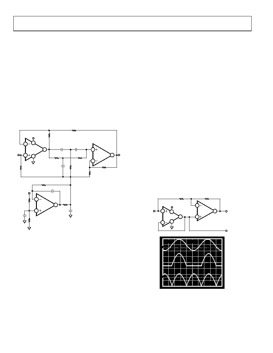
3 V, 50 HZ/60 HZ ACTIVE NOTCH FILTER WITH
FALSE GROUND
The filter section uses a pair of OP491s in a twin-T
configuration whose frequency selectivity is very sensitive
to the relative matching of the capacitors and resistors in
the twin-T section. Mylar is the material of choice for the
capacitors, and the relative matching of the capacitors and
resistors determines the pass band symmetry of the filter. Using
1% resistors and 5% capacitors produces satisfactory results.
To process ac signals in a single-supply system, it is often best
to use a false ground biasing scheme. Figure 72 illustrates a
circuit that uses this approach. In this circuit, a false-ground
circuit biases an active notch filter used to reject 50 Hz/60 Hz
power line interference in portable patient monitoring
equipment. Notch filters are quite commonly used to reject
power line frequency interference that often obscures low
frequency physiological signals, such as heart rates, blood
pressure readings, EEGs, and EKGs. This notch filter effectively
squelches 60 Hz pickup at a filter Q of 0.75. Substituting
3.16 kΩ resistors for the 2.67 kΩ resistors in the twin-T section
(R1 through R5) configures the active filter to reject 50 Hz
interference.
SINGLE-SUPPLY, HALF-WAVE, AND FULL-WAVE
RECTIFIERS
An OPx91 device configured as a voltage follower operating on
a single supply can be used as a simple half-wave rectifier in low
frequency (<2 kHz) applications. A full-wave rectifier can be
configured with a pair of OP291s, as illustrated in Figure 73.
The circuit works in the following way. When the input signal is
above 0 V, the output of Amplifier A1 follows the input signal.
Because the noninverting input of Amplifier A2 is connected to
the output of A1, op amp loop control forces the inverting input
of the A2 to the same potential. The result is that both terminals
of R1 are equipotential; that is, no current flows. Because there
is no current flow in R1, the same condition exists for R2; thus,
the output of the circuit tracks the input signal. When the input
signal is below 0 V, the output voltage of A1 is forced to 0 V.
This condition now forces A2 to operate as an inverting voltage
follower because the noninverting terminal of A2 is also at 0 V.
The output voltage at VOUTA is then a full-wave rectified version
of the input signal. If needed, a buffered, half-wave rectified
version of the input signal is available at VOUTB.
R11
100k
VOUT
R1
2.67k
R3
2.67k
A1
1/4
OP491
3V
VIN
R6
100k
0.01μF
C5
A3
R12
499
C6
1.5V
1μF
3V
R9
1M
R10
1M
C4
1μF
C2
R4
2.67k
A2
R5
1.33k
(2.67k ÷ 2)
R7
1k
R8
1k
C1
1μF1μF
R2
2.67k
1
2
4
3
11
1/4
OP491
7
6
5
9
1/4
OP491
10
8
00
29
4-
07
6
C3
2μF
(1μF × 2)
10
(1V/DIV)
(0.5V/DIV)
TIME (200μs/DIV)
R1
100k
A1
5V
VIN
2V p-p
<2kHz
R2
100k
1/2
OP291
A2
VOUTA
VOUTB
FULL-WAVE
RECTIFIED
OUTPUT
HALF-WAVE
RECTIFIED
OUTPUT
6
7
5
1/2
OP291
2
1
3
4
8
1V
500mV
VOUTA
VIN
VOUTB
90
100
0%
00
29
4-
0
77
500mV
200μs
Figure 72. A 3 V Single-Supply, 50 Hz/60 Hz Active Notch Filter
with False Ground
Amplifier A3 is the heart of the false ground bias circuit.
It buffers the voltage developed by R9 and R10 and is the
reference for the active notch filter. Because the OP491
exhibits a rail-to-rail input common-mode range, R9 and R10
are chosen to split the 3 V supply symmetrically. An in-the-loop
compensation scheme used around the OP491 allows the op
amp to drive C6, a 1 μF capacitor, without oscillation. C6
maintains a low impedance ac ground over the operating
frequency range of the filter.
Figure 73. Single-Supply, Half-Wave, and Full-Wave Rectifiers
Using an OP291
相关PDF资料 |
PDF描述 |
|---|---|
| FTSH-108-01-L-DH | CONN HEADR 16POS DL .05" R/A SMD |
| EL8401IUZ-T7 | IC OP AMP 200MHZ R-R 16-QSOP |
| TMM-119-01-G-S-SM | CONN HEADER 19POS SNGL 2MM SMD |
| TLW-122-06-T-D | CONN HEADER .100" 44POS DUAL TIN |
| ADA4091-2ARZ-R7 | IC OPAMP GP R-R 1.27MHZ 8SOIC |
相关代理商/技术参数 |
参数描述 |
|---|---|
| OP291GSZ | 功能描述:IC OPAMP GP R-R 3MHZ DUAL 8SOIC RoHS:是 类别:集成电路 (IC) >> Linear - Amplifiers - Instrumentation 系列:- 标准包装:2,500 系列:- 放大器类型:通用 电路数:4 输出类型:- 转换速率:0.6 V/µs 增益带宽积:1MHz -3db带宽:- 电流 - 输入偏压:45nA 电压 - 输入偏移:2000µV 电流 - 电源:1.4mA 电流 - 输出 / 通道:40mA 电压 - 电源,单路/双路(±):3 V ~ 32 V,±1.5 V ~ 16 V 工作温度:0°C ~ 70°C 安装类型:表面贴装 封装/外壳:14-TSSOP(0.173",4.40mm 宽) 供应商设备封装:14-TSSOP 包装:带卷 (TR) 其它名称:LM324ADTBR2G-NDLM324ADTBR2GOSTR |
| OP291GSZ-REEL | 功能描述:IC OPAMP GP R-R 3MHZ DUAL 8SOIC RoHS:是 类别:集成电路 (IC) >> Linear - Amplifiers - Instrumentation 系列:- 标准包装:50 系列:LinCMOS™ 放大器类型:通用 电路数:4 输出类型:- 转换速率:0.05 V/µs 增益带宽积:110kHz -3db带宽:- 电流 - 输入偏压:0.7pA 电压 - 输入偏移:210µV 电流 - 电源:57µA 电流 - 输出 / 通道:30mA 电压 - 电源,单路/双路(±):3 V ~ 16 V,±1.5 V ~ 8 V 工作温度:-40°C ~ 85°C 安装类型:表面贴装 封装/外壳:14-SOIC(0.154",3.90mm 宽) 供应商设备封装:14-SOIC 包装:管件 产品目录页面:865 (CN2011-ZH PDF) 其它名称:296-1834296-1834-5 |
| OP291GSZ-REEL7 | 功能描述:IC OPAMP GP R-R 3MHZ DUAL 8SOIC RoHS:是 类别:集成电路 (IC) >> Linear - Amplifiers - Instrumentation 系列:- 其它有关文件:Automotive Product Guide 产品培训模块:Lead (SnPb) Finish for COTS Obsolescence Mitigation Program 标准包装:1 系列:- 放大器类型:通用 电路数:1 输出类型:满摆幅 转换速率:3 V/µs 增益带宽积:10MHz -3db带宽:- 电流 - 输入偏压:1pA 电压 - 输入偏移:70µV 电流 - 电源:2.5mA 电流 - 输出 / 通道:48mA 电压 - 电源,单路/双路(±):2.7 V ~ 5.5 V,±1.35 V ~ 2.75 V 工作温度:-40°C ~ 125°C 安装类型:表面贴装 封装/外壳:SOT-23-6 供应商设备封装:SOT-6 包装:Digi-Reel® 其它名称:MAX4475AUT#TG16DKR |
| OP292 | 制造商:AD 制造商全称:Analog Devices 功能描述:DUAL/QUAD SINGLE SUPPLY OPERATIONAL AMPLIFIER |
| OP-292 | 制造商:AD 制造商全称:Analog Devices 功能描述:DUAL/QUAD SINGLE SUPPLY OPERATIONAL AMPLIFIER |
发布紧急采购,3分钟左右您将得到回复。