参数资料
| 型号: | OP291GSZ |
| 厂商: | Analog Devices Inc |
| 文件页数: | 13/24页 |
| 文件大小: | 0K |
| 描述: | IC OPAMP GP R-R 3MHZ DUAL 8SOIC |
| 标准包装: | 98 |
| 放大器类型: | 通用 |
| 电路数: | 2 |
| 输出类型: | 满摆幅 |
| 转换速率: | 0.5 V/µs |
| 增益带宽积: | 3MHz |
| 电流 - 输入偏压: | 30nA |
| 电压 - 输入偏移: | 80µV |
| 电流 - 电源: | 260µA |
| 电流 - 输出 / 通道: | 16mA |
| 电压 - 电源,单路/双路(±): | 2.7 V ~ 12 V,±1.35 V ~ 6 V |
| 工作温度: | -40°C ~ 125°C |
| 安装类型: | 表面贴装 |
| 封装/外壳: | 8-SOIC(0.154",3.90mm 宽) |
| 供应商设备封装: | 8-SO |
| 包装: | 管件 |
| 产品目录页面: | 768 (CN2011-ZH PDF) |
OP191/OP291/OP491
Rev. E | Page 20 of 24
A 2.5 V REFERENCE FROM A 3 V SUPPLY
In many single-supply applications, the need for a 2.5 V
reference often arises. Many commercially available monolithic
2.5 V references require a minimum operating supply voltage of
4 V. The problem is exacerbated when the minimum operating
system supply voltage is 3 V. The circuit illustrated in Figure 67
is an example of a 2.5 V reference that operates from a single
3 V supply. The circuit takes advantage of the OP291 rail-to-rail
input and output voltage ranges to amplify an AD589 1.235 V
output to 2.5 V. The OP291 low TCVOS of 1 μV/°C helps
maintain an output voltage temperature coefficient of less than
200 ppm/°C. The circuit overall temperature coefficient is
dominated by the temperature coefficient of R2 and R3. Lower
temperature coefficient resistors are recommended. The entire
circuit draws less than 420 μA from a 3 V supply at 25°C.
RESISTORS = 1%, 100ppm/°C
POTENTIOMETER = 10 TURN, 100ppm/°C
R3
100k
1/2
OP291
R2
100k
3V
R1
5k
2.5V
REF
R1
17.4k
AD589
3V
3
2
1
8
4
00
29
4-
0
71
Figure 67. A 2.5 V Reference that Operates on a Single 3 V Supply
5 V ONLY, 12-BIT DAC SWINGS RAIL-TO-RAIL
The OPx91 family is ideal for use with a CMOS DAC to
generate a digitally controlled voltage with a wide output range.
Figure 68 shows the DAC8043 used in conjunction with the
AD589 to generate a voltage output from 0 V to 1.23 V. The
DAC is operated in voltage switching mode, where the reference
is connected to the current output, IOUT, and the output voltage
is taken from the VREF pin. This topology is inherently
noninverting as opposed to the classic current output mode,
which is inverting and, therefore, unsuitable for single supply.
5V
R1
17.8k
AD589
R2
R3
R4
232
1%
32.4k
1%
100k
1%
VOUT = –––– (5V)
D
4096
GND CLK SR1
47
6
5
DIGITAL
CONTROL
LD
VREF
RFB
VDD
IOUT
2
3
8
1.23V
5V
DAC8043
1/2
OP291
3
2
1
8
4
1
00294-
072
Figure 68. 5 V Only, 12-Bit DAC Swings Rail-to-Rail
The OP291 serves two functions. First, it is required to buffer
the high output impedance of the DAC VREF pin, which is on the
order of 10 kΩ. The op amp provides a low impedance output
to drive any following circuitry. Second, the op amp amplifies
the output signal to provide a rail-to-rail output swing. In this
particular case, the gain is set to 4.1 to generate a 5.0 V output
when the DAC is at full scale. If other output voltage ranges are
needed, such as 0 V to 4.095 V, the gain can easily be adjusted
by altering the value of the resistors.
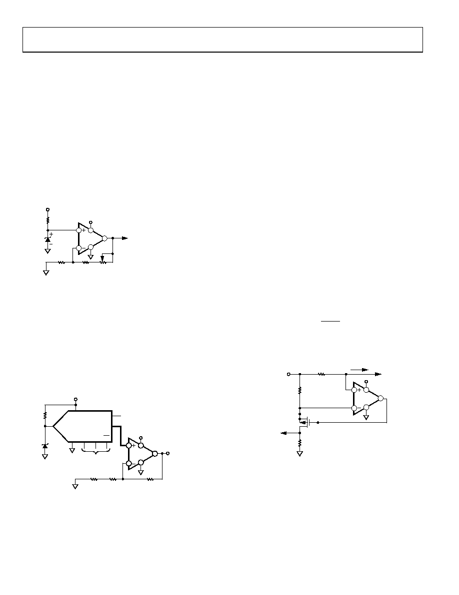
A HIGH-SIDE CURRENT MONITOR
In the design of power supply control circuits, a great deal of
design effort is focused on ensuring a pass transistor’s long-
term reliability over a wide range of load current conditions.
As a result, monitoring and limiting device power dissipation
is of prime importance in these designs. The circuit illustrated
in Figure 69 is an example of a 5 V, single-supply, high-side
current monitor that can be incorporated into the design of a
voltage regulator with fold-back current limiting or a high
current power supply with crowbar protection. This design uses
an OP291 rail-to-rail input voltage range to sense the voltage
drop across a 0.1 Ω current shunt. A p-channel MOSFET used
as the feedback element in the circuit converts the op amp
differential input voltage into a current. This current is then
applied to R2 to generate a voltage that is a linear representation
of the load current. The transfer equation for the current
monitor is given by
L
SENSE
I
R
Output
Monitor
×
×
=
1
2
For the element values shown, the monitor output transfer
characteristic is 2.5 V/A.
5V
RSENSE
0.1
5V
IL
S
G
M1
3N163
D
R2
2.49k
MONITOR
OUTPUT
R1
100
1/2
OP291
3
2
1
8
4
00
29
4-
07
3
Figure 69. A High-Side Load Current Monitor
相关PDF资料 |
PDF描述 |
|---|---|
| 9-146304-0-05 | CONN HEADR BRKWAY .100 05POS R/A |
| 1SMC5.0AT3G | TVS ZENER UNIDIR 1500W 5.0V SMC |
| N3627-6202RB | CONN HEADER 24PS STR SHORT LATCH |
| N3627-5302RB | CONN HEADER 24PS R/A LONG LATCH |
| TSW-150-23-L-S | CONN HEADER 50POS .100" SGL GOLD |
相关代理商/技术参数 |
参数描述 |
|---|---|
| OP291GSZ-REEL | 功能描述:IC OPAMP GP R-R 3MHZ DUAL 8SOIC RoHS:是 类别:集成电路 (IC) >> Linear - Amplifiers - Instrumentation 系列:- 标准包装:50 系列:LinCMOS™ 放大器类型:通用 电路数:4 输出类型:- 转换速率:0.05 V/µs 增益带宽积:110kHz -3db带宽:- 电流 - 输入偏压:0.7pA 电压 - 输入偏移:210µV 电流 - 电源:57µA 电流 - 输出 / 通道:30mA 电压 - 电源,单路/双路(±):3 V ~ 16 V,±1.5 V ~ 8 V 工作温度:-40°C ~ 85°C 安装类型:表面贴装 封装/外壳:14-SOIC(0.154",3.90mm 宽) 供应商设备封装:14-SOIC 包装:管件 产品目录页面:865 (CN2011-ZH PDF) 其它名称:296-1834296-1834-5 |
| OP291GSZ-REEL7 | 功能描述:IC OPAMP GP R-R 3MHZ DUAL 8SOIC RoHS:是 类别:集成电路 (IC) >> Linear - Amplifiers - Instrumentation 系列:- 其它有关文件:Automotive Product Guide 产品培训模块:Lead (SnPb) Finish for COTS Obsolescence Mitigation Program 标准包装:1 系列:- 放大器类型:通用 电路数:1 输出类型:满摆幅 转换速率:3 V/µs 增益带宽积:10MHz -3db带宽:- 电流 - 输入偏压:1pA 电压 - 输入偏移:70µV 电流 - 电源:2.5mA 电流 - 输出 / 通道:48mA 电压 - 电源,单路/双路(±):2.7 V ~ 5.5 V,±1.35 V ~ 2.75 V 工作温度:-40°C ~ 125°C 安装类型:表面贴装 封装/外壳:SOT-23-6 供应商设备封装:SOT-6 包装:Digi-Reel® 其它名称:MAX4475AUT#TG16DKR |
| OP292 | 制造商:AD 制造商全称:Analog Devices 功能描述:DUAL/QUAD SINGLE SUPPLY OPERATIONAL AMPLIFIER |
| OP-292 | 制造商:AD 制造商全称:Analog Devices 功能描述:DUAL/QUAD SINGLE SUPPLY OPERATIONAL AMPLIFIER |
| OP292_02 | 制造商:AD 制造商全称:Analog Devices 功能描述:Dual/Quad Single-Supply Operational Amplifiers |
发布紧急采购,3分钟左右您将得到回复。