- 您现在的位置:买卖IC网 > PDF目录3439 > OP462HRU-REEL (Analog Devices Inc)IC OPAMP GP R-R 15MHZ LN 14TSSOP PDF资料下载
参数资料
| 型号: | OP462HRU-REEL |
| 厂商: | Analog Devices Inc |
| 文件页数: | 4/20页 |
| 文件大小: | 0K |
| 描述: | IC OPAMP GP R-R 15MHZ LN 14TSSOP |
| 标准包装: | 2,500 |
| 放大器类型: | 通用 |
| 电路数: | 4 |
| 输出类型: | 满摆幅 |
| 转换速率: | 13 V/µs |
| 增益带宽积: | 15MHz |
| 电流 - 输入偏压: | 260nA |
| 电压 - 输入偏移: | 25µV |
| 电流 - 电源: | 550µA |
| 电流 - 输出 / 通道: | 30mA |
| 电压 - 电源,单路/双路(±): | 2.7 V ~ 12 V,±1.35 V ~ 6 V |
| 工作温度: | -40°C ~ 125°C |
| 安装类型: | 表面贴装 |
| 封装/外壳: | 14-TSSOP(0.173",4.40mm 宽) |
| 供应商设备封装: | 14-TSSOP |
| 包装: | 带卷 (TR) |
OP162/OP262/OP462
Data Sheet
Rev. H | Page 12 of 20
APPLICATIONS
FUNCTIONAL DESCRIPTION
The OPx62 family is fabricated using Analog Devices’ high
speed complementary bipolar process, also called XFCB. This
process trench isolates each transistor to lower parasitic capaci-
tances for high speed performance. This high speed process has
been implemented without sacrificing the excellent transistor
matching and overall dc performance characteristic of Analog
Devices’ complementary bipolar process. This makes the OPx62
family an excellent choice as an extremely fast and accurate low
voltage op amp.
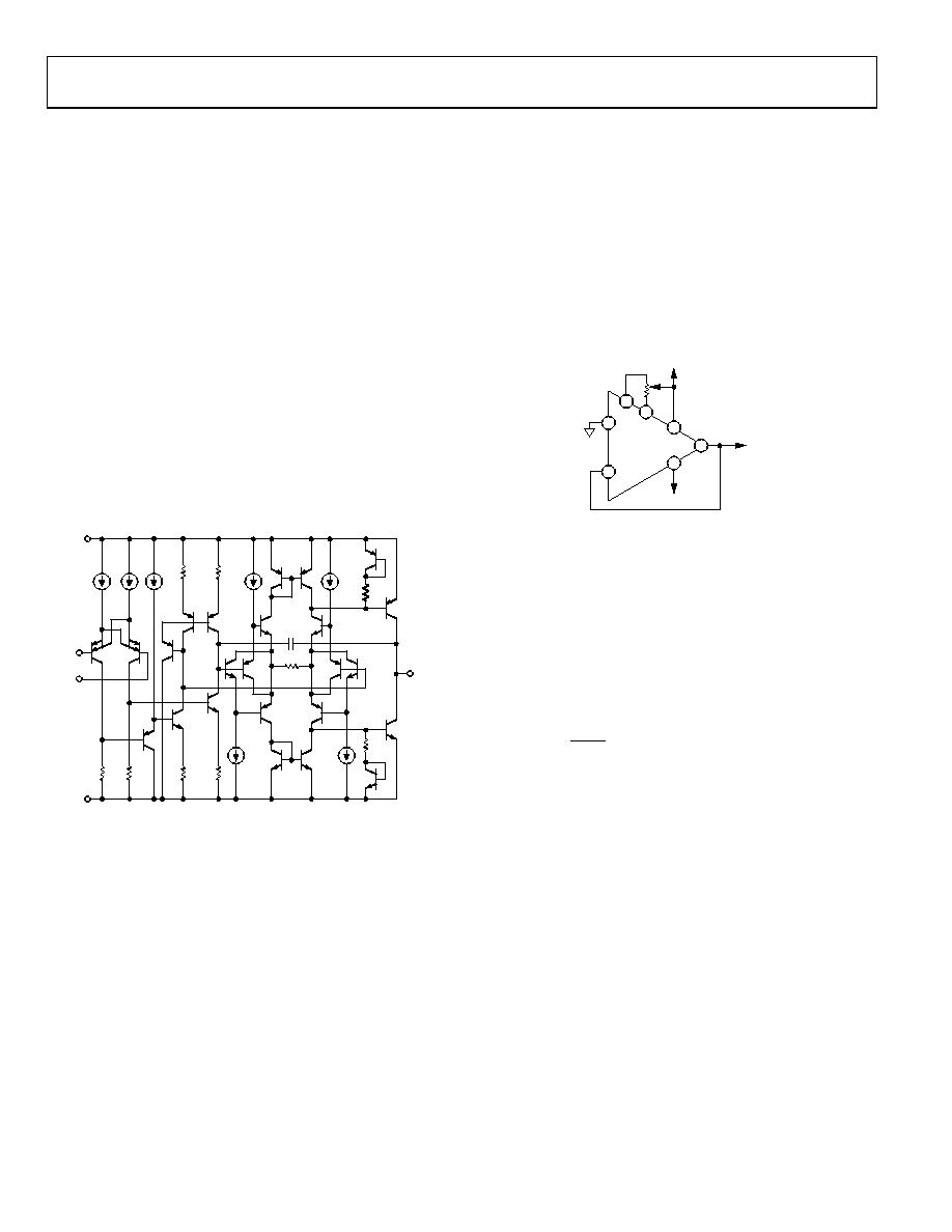
Figure 30 shows a simplified equivalent schematic for the OP162.
A PNP differential pair is used at the input of the device. The
cross connecting of the emitters lowers the transconductance of
the input stage improving the slew rate of the device. Lowering
the transconductance through cross connecting the emitters has
another advantage in that it provides a lower noise factor than if
emitter degeneration resistors were used. The input stage can
function with the base voltages taken all the way to the negative
power supply, or up to within 1 V of the positive power supply.
Figure 30. Simplified Schematic
Two complementary transistors in a common-emitter
configuration are used for the output stage. This allows the
output of the device to swing to within 50 mV of either supply
rail at load currents less than 1 mA. As load current increases,
the maximum voltage swing of the output decreases. This is due
to the collector-to-emitter saturation voltages of the output
transistors increasing. The gain of the output stage, and conse-
quently the open-loop gain of the amplifier, is dependent on the
load resistance connected at the output. Because the dominant pole
frequency is inversely proportional to the open-loop gain, the
unity-gain bandwidth of the device is not affected by the load
resistance. This is typically the case in rail-to-rail output
devices.
OFFSET ADJUSTMENT
Because the OP162/OP262/OP462 have an exceptionally low
typical offset voltage, adjustment to correct offset voltage may
not be needed. However, the OP162 has pinouts to attach a
nulling resistor. Figure 31 shows how the OP162 offset voltage
can be adjusted by connecting a potentiometer between Pin 1
and Pin 8, and connecting the wiper to VCC. It is important to
avoid accidentally connecting the wiper to VEE, as this can damage
the device. The recommended value for the potentiometer is
20 k.
Figure 31. Offset Adjustment Schematic
RAIL-TO-RAIL OUTPUT
The OP162/OP262/OP462 have a wide output voltage range
that extends to within 60 mV of each supply rail with a load
current of 5 mA. Decreasing the load current extends the output
voltage range even closer to the supply rails. The common-mode
input range extends from ground to within 1 V of the positive
supply. It is recommended that there be some minimal amount
of gain when a rail-to-rail output swing is desired. The minimum
gain required is based on the supply voltage and can be found as
1
=
S
V,min
V
A
where VS is the positive supply voltage. With a single-supply
voltage of 5 V, the minimum gain to achieve rail-to-rail output
should be 1.25.
OUTPUT SHORT-CIRCUIT PROTECTION
To achieve a wide bandwidth and high slew rate, the output of
the OP162/OP262/OP462 are not short-circuit protected. Shorting
the output directly to ground or to a supply rail may destroy the
device. The typical maximum safe output current is ±30 mA.
Steps should be taken to ensure the output of the device will not
be forced to source or sink more than 30 mA.
In applications where some output current protection is needed,
but not at the expense of reduced output voltage headroom, a
low value resistor in series with the output can be used. This is
shown in Figure 32. The resistor is connected within the feed-
back loop of the amplifier so that if VOUT is shorted to ground
VCC
VEE
+IN
–IN
VOUT
00288-033
–5V
20k
OP162
+5V
VOS
3
2
4
7
8
1
6
00288-034
相关PDF资料 |
PDF描述 |
|---|---|
| 0034.3412 | FUSE 315MA 250VAC 6X32 SLOW |
| 0034.3425 | FUSE 6.3A 250VAC 6X32 SLOW |
| 0034.3418 | FUSE 1.25A 250VAC 6X32 SLOW |
| LR2010-R15FW | RES 0.15 OHM 1.0W 2010 1% SMD |
| 0034.3422 | FUSE 3.15A 250VAC 6X32 SLOW |
相关代理商/技术参数 |
参数描述 |
|---|---|
| OP462HRUZ-REEL | 功能描述:IC OPAMP QUAD R-R 15MHZ 14-TSSOP RoHS:是 类别:集成电路 (IC) >> Linear - Amplifiers - Instrumentation 系列:- 标准包装:2,500 系列:- 放大器类型:通用 电路数:4 输出类型:- 转换速率:0.6 V/µs 增益带宽积:1MHz -3db带宽:- 电流 - 输入偏压:45nA 电压 - 输入偏移:2000µV 电流 - 电源:1.4mA 电流 - 输出 / 通道:40mA 电压 - 电源,单路/双路(±):3 V ~ 32 V,±1.5 V ~ 16 V 工作温度:0°C ~ 70°C 安装类型:表面贴装 封装/外壳:14-TSSOP(0.173",4.40mm 宽) 供应商设备封装:14-TSSOP 包装:带卷 (TR) 其它名称:LM324ADTBR2G-NDLM324ADTBR2GOSTR |
| OP467 | 制造商:AD 制造商全称:Analog Devices 功能描述:Quad Precision, High Speed Operational Amplifier |
| OP467_07 | 制造商:AD 制造商全称:Analog Devices 功能描述:Quad Precision, High Speed Operational Amplifier |
| OP467ARC/883 | 制造商:AD 制造商全称:Analog Devices 功能描述:Quad Precision, High Speed Operational Amplifier |
发布紧急采购,3分钟左右您将得到回复。