参数资料
| 型号: | OP467GPZ |
| 厂商: | Analog Devices Inc |
| 文件页数: | 5/20页 |
| 文件大小: | 0K |
| 描述: | IC OPAMP GP 28MHZ QUAD 14DIP |
| 标准包装: | 25 |
| 放大器类型: | 通用 |
| 电路数: | 4 |
| 转换速率: | 350 V/µs |
| 增益带宽积: | 28MHz |
| 电流 - 输入偏压: | 150nA |
| 电压 - 输入偏移: | 200µV |
| 电流 - 电源: | 8mA |
| 电压 - 电源,单路/双路(±): | ±4.5 V ~ 18 V |
| 工作温度: | -40°C ~ 85°C |
| 安装类型: | 通孔 |
| 封装/外壳: | 14-DIP(0.300",7.62mm) |
| 供应商设备封装: | 14-PDIP |
| 包装: | 管件 |
| 产品目录页面: | 770 (CN2011-ZH PDF) |
OP467
Rev. | Page 13 of 20
APPLICATIONS INFORMATION
OUTPUT SHORT-CIRCUIT PERFORMANCE
To achieve a wide bandwidth and high slew rate, the OP467
output is not short-circuit protected. Shorting the output to
ground or to the supplies may destroy the device.
For safe operation, the output load current should be limited so
that the junction temperature does not exceed the absolute
maximum junction temperature.
The maximum internal power dissipation can be calculated by
JA
D
P
θ
=
A
J
T
max
where:
TJ and TA are junction and ambient temperatures, respectively.
PD is device internal power dissipation.
θJA is the packaged device thermal resistance given in the data sheet.
UNUSED AMPLIFIERS
It is recommended that any unused amplifiers in the quad
package be connected as a unity-gain follower with a 1 kΩ
feedback resistor with noninverting input tied to the ground plain.
PCB LAYOUT CONSIDERATIONS
Satisfactory performance of a high speed op amp largely
depends on a good PCB layout. To achieve the best dynamic
performance, follow the high frequency layout technique.
GROUNDING
A good ground plain is essential to achieve the optimum
performance in high speed applications. It can significantly
reduce the undesirable effects of ground loops and IR drops by
providing a low impedance reference point. Best results are
obtained with a multilayer board design with one layer assigned
to the ground plain. To maintain a continuous and low impedance
ground, avoid running any traces on this layer.
POWER SUPPLY CONSIDERATIONS
In high frequency circuits, device lead length introduces an
inductance in series with the circuit. This inductance, combined
with stray capacitance, forms a high frequency resonance circuit.
Poles generated by these circuits cause gain peaking and additional
phase shift, reducing the phase margin of the op amp and leading
to an unstable operation.
A practical solution to this problem is to reduce the resonance
frequency low enough to take advantage of the power supply
rejection of the amplifier. This is easily done by placing capacitors
across the supply line and the ground plane as close as possible
to the device pin. Because capacitors also have internal parasitic
components, such as stray inductance, selecting the right capacitor
is important. To be effective, they should have low impedance
over the frequency range of interest. Tantalum capacitors are an
excellent choice for their high capacitance/size ratio, but their
effective series resistance (ESR) increases with frequency
making them less effective.
On the other hand, ceramic chip capacitors have excellent ESR
and effective series inductance (ESL) performance at higher
frequencies, and because of their small size, they can be placed
very close to the device pin, further reducing the stray inductance.
Best results are achieved by using a combination of these two
capacitors. A 5 μF to 10 μF tantalum parallel capacitor with a
0.1 μF ceramic chip capacitor is recommended. If additional
isolation from high frequency resonances of the power supply is
needed, a ferrite bead should be placed in series with the supply
lines between the bypass capacitors and the power supply. Note
that addition of the ferrite bead introduces a new pole and zero
to the frequency response of the circuit and could cause unstable
operation if it is not selected properly.
00
30
2-
04
0
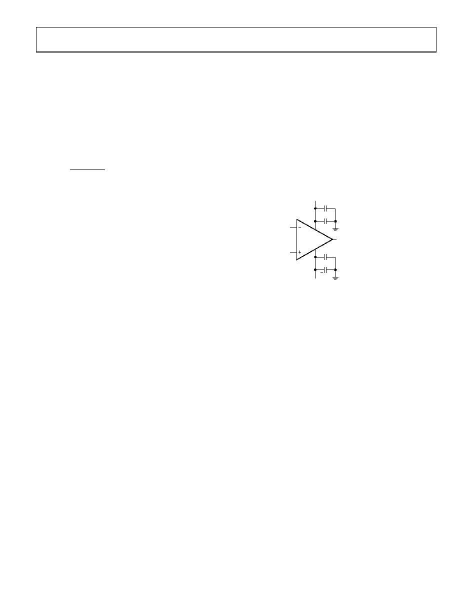
+VS
+
10F TANTALUM
0.1F CERAMIC CHIP
–VS
10F TANTALUM
0.1F CERAMIC CHIP
Figure 40. Recommended Power Supply Bypass
SIGNAL CONSIDERATIONS
Input and output traces need special attention to assure a
minimum stray capacitance. Input nodes are very sensitive to
capacitive reactance, particularly when connected to a high
impedance circuit. Stray capacitance can inject undesirable
signals from a noisy line into a high impedance input. Protect
high impedance input traces by providing guard traces around
them, which also improves the channel separation significantly.
Additionally, any stray capacitance in parallel with the input
capacitance of the op amp generates a pole in the frequency
response of the circuit. The additional phase shift caused by this
pole reduces the gain margin of the circuit. If this pole is within
the gain range of the op amp, it causes unstable performance. To
reduce these undesirable effects, use the lowest impedance
where possible. Lowering the impedance at this node places the
poles at a higher frequency, far above the gain range of the
amplifier. Stray capacitance on the PCB can be reduced by making
the traces narrow and as short as possible. Further reduction
can be realized by choosing a smaller pad size, increasing the
spacing between the traces, and using PCB material with a low
dielectric constant insulator (dielectric constant of some common
insulators: air = 1, Teflon = 2.2, and FR4 = 4.7, with air being
an ideal insulator).
Removing segments of the ground plane directly under the
input and output pads is recommended.
相关PDF资料 |
PDF描述 |
|---|---|
| TSW-128-08-T-S-RA | CONN HEADER 28POS .100" SNGL R/A |
| LT1359CS#PBF | IC OP-AMP HISPD 25MHZ QUAD16SOIC |
| TSW-109-05-T-D | CONN HEADER 18POS .100" DL TIN |
| AD621BNZ | IC AMP INST LDRIFT LP 18MA 8DIP |
| 929500-01-21-RK | CONN HEADER .100 SNGL R/A 21POS |
相关代理商/技术参数 |
参数描述 |
|---|---|
| OP467GS | 功能描述:IC OPAMP GP 28MHZ QUAD 16SOIC RoHS:否 类别:集成电路 (IC) >> Linear - Amplifiers - Instrumentation 系列:- 标准包装:50 系列:- 放大器类型:J-FET 电路数:2 输出类型:- 转换速率:3.5 V/µs 增益带宽积:1MHz -3db带宽:- 电流 - 输入偏压:30pA 电压 - 输入偏移:2000µV 电流 - 电源:200µA 电流 - 输出 / 通道:- 电压 - 电源,单路/双路(±):7 V ~ 36 V,±3.5 V ~ 18 V 工作温度:0°C ~ 70°C 安装类型:通孔 封装/外壳:8-DIP(0.300",7.62mm) 供应商设备封装:8-PDIP 包装:管件 |
| OP467GS-REEL | 功能描述:IC OPAMP GP 28MHZ QUAD 16SOIC RoHS:否 类别:集成电路 (IC) >> Linear - Amplifiers - Instrumentation 系列:- 标准包装:2,500 系列:Excalibur™ 放大器类型:J-FET 电路数:1 输出类型:- 转换速率:45 V/µs 增益带宽积:10MHz -3db带宽:- 电流 - 输入偏压:20pA 电压 - 输入偏移:490µV 电流 - 电源:1.7mA 电流 - 输出 / 通道:48mA 电压 - 电源,单路/双路(±):4.5 V ~ 38 V,±2.25 V ~ 19 V 工作温度:-40°C ~ 85°C 安装类型:表面贴装 封装/外壳:8-SOIC(0.154",3.90mm 宽) 供应商设备封装:8-SOIC 包装:带卷 (TR) |
| OP467GSZ | 功能描述:IC OPAMP GP 28MHZ QUAD 16SOIC RoHS:是 类别:集成电路 (IC) >> Linear - Amplifiers - Instrumentation 系列:- 标准包装:2,500 系列:- 放大器类型:通用 电路数:4 输出类型:- 转换速率:0.6 V/µs 增益带宽积:1MHz -3db带宽:- 电流 - 输入偏压:45nA 电压 - 输入偏移:2000µV 电流 - 电源:1.4mA 电流 - 输出 / 通道:40mA 电压 - 电源,单路/双路(±):3 V ~ 32 V,±1.5 V ~ 16 V 工作温度:0°C ~ 70°C 安装类型:表面贴装 封装/外壳:14-TSSOP(0.173",4.40mm 宽) 供应商设备封装:14-TSSOP 包装:带卷 (TR) 其它名称:LM324ADTBR2G-NDLM324ADTBR2GOSTR |
| OP467GSZ-REEL | 功能描述:IC OPAMP GP 28MHZ QUAD 16SOIC RoHS:是 类别:集成电路 (IC) >> Linear - Amplifiers - Instrumentation 系列:- 标准包装:2,500 系列:Excalibur™ 放大器类型:J-FET 电路数:1 输出类型:- 转换速率:45 V/µs 增益带宽积:10MHz -3db带宽:- 电流 - 输入偏压:20pA 电压 - 输入偏移:490µV 电流 - 电源:1.7mA 电流 - 输出 / 通道:48mA 电压 - 电源,单路/双路(±):4.5 V ~ 38 V,±2.25 V ~ 19 V 工作温度:-40°C ~ 85°C 安装类型:表面贴装 封装/外壳:8-SOIC(0.154",3.90mm 宽) 供应商设备封装:8-SOIC 包装:带卷 (TR) |
| OP470 | 制造商:AD 制造商全称:Analog Devices 功能描述:Very Low Noise Quad Operational Amplifier |
发布紧急采购,3分钟左右您将得到回复。