参数资料
| 型号: | OP470EY |
| 厂商: | Analog Devices Inc |
| 文件页数: | 2/16页 |
| 文件大小: | 0K |
| 描述: | IC OPAMP GP 6MHZ QUAD LN 14CDIP |
| 标准包装: | 25 |
| 放大器类型: | 通用 |
| 电路数: | 4 |
| 转换速率: | 2 V/µs |
| 增益带宽积: | 6MHz |
| 电流 - 输入偏压: | 6nA |
| 电压 - 输入偏移: | 100µV |
| 电流 - 电源: | 9mA |
| 电压 - 电源,单路/双路(±): | 9 V ~ 36 V,±4.5 V ~ 18 V |
| 工作温度: | -25°C ~ 85°C |
| 安装类型: | 通孔 |
| 封装/外壳: | 14-CDIP(0.300",7.62mm) |
| 供应商设备封装: | 14-CERDIP |
| 包装: | 管件 |
| 产品目录页面: | 772 (CN2011-ZH PDF) |
REV. B
OP470
–10–
Figure 6 shows peak-to-peak noise versus source resistance over
the 0.1 Hz to 10 Hz range. Once again, at low values of RS, the
voltage noise of the OP470 is the major contributor to peak-to-peak
noise with current noise the major contributor as RS increases.
The crossover point between the OP470 and the OP400 for
peak-to-peak noise is at RS = 17 k
W.
The OP471 is a higher speed version of the OP470, with a slew
rate of 8 V/
ms. Noise of the OP471 is only slightly higher than
the OP470. Like the OP470, the OP471 is unity-gain stable.
RS – SOURCE RESISTANCE –
1000
10
100
100k
PEAK-T
O-PEAK
NOISE
–
nV/
Hz
100
10k
1k
OP11
OP400
OP471
OP470
RESISTOR
NOISE ONLY
Figure 6. Peak-To-Peak Noise (0.1 Hz to 10 Hz) vs. Source
Resistance (Includes Resistor Noise)
For reference, typical source resistances of some signal sources
are listed in Table I.
R1
5
R3
1.24k
OP470
DUT
R2
5
R5
909
OP27E
R4
200
C1
2 F
R6
600k
R9
306k
OP15E
R8
10k
D1
1N4148
D2
1N4148
C2
0.032 F
R10
65.4k
R11
65.4k
C3
0.22 F
OP15E
C4
0.22 F
R13
5.9k
R12
10k
R14
4.99k
C5
1 F
eOUT
GAIN = 50,000
VS = 5V
Figure 7. Peak-To-Peak Voltage Noise Test Circuit (0.1 Hz to 10 Hz)
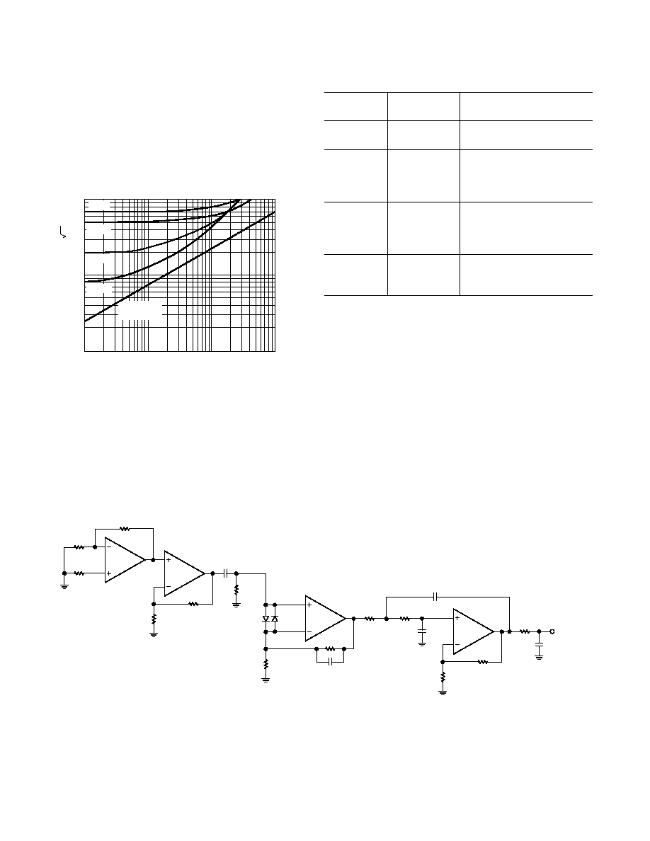
Table I.
Device
Source
Impedance
Comments
Strain gage
<500
W
Typically used in
low frequency applications.
Magnetic
<1500
W
Low IB very important to reduce
tapehead
self-magnetization problems
when direct coupling is used.
OP470 IB can be neglected.
Magnetic
<1500
W
Similar need for low IB in direct
phonograph
coupled applications. OP470
cartridges
will not introduce any self-
magnetization problem.
Linear variable <1500
W
Used in rugged servo-feedback
differential
applications. Bandwidth of
transformer
interest is 400 Hz to 5 kHz.
For further information regarding noise calculations, see “Minimization of Noise
in Op Amp Applications,” Application Note AN-15.
NOISE MEASUREMENTS—
PEAK-TO-PEAK VOLTAGE NOISE
The circuit of Figure 7 is a test setup for measuring peak-to-peak
voltage noise. To measure the 200 nV peak-to-peak noise speci-
fication of the OP470 in the 0.1 Hz to 10 Hz range, the following
precautions must be observed:
1. The device must be warmed up for at least five minutes. As
shown in the warm-up drift curve, the offset voltage typi-
cally changes 5
mV due to increasing chip temperature after
power-up. In the 10-second measurement interval, these
temperature-induced effects can exceed tens of nanovolts.
2. For similar reasons, the device must be well-shielded from
air currents. Shielding also minimizes thermocouple effects.
3. Sudden motion in the vicinity of the device can also “feedthrough”
to increase the observed noise.
相关PDF资料 |
PDF描述 |
|---|---|
| 929836-02-04-RK | CONN HEADER .100 DUAL STR 8POS |
| OP400EY | IC OPAMP GP 500KHZ QUAD 14CDIP |
| 929835-01-26-RK | CONN HEADER .100 SNGL R/A 26POS |
| LT2079AIS#PBF | IC OPAMP MICROPOWER QUAD 14SOIC |
| 929834-05-15-RK | CONN HEADER .100 SNGL STR 15POS |
相关代理商/技术参数 |
参数描述 |
|---|---|
| OP-470EY | 制造商:AD 制造商全称:Analog Devices 功能描述:VERY LOW NOISE QUAD OPERATIONAL AMPLIFIER |
| OP470FY | 制造商:Analog Devices 功能描述: |
| OP-470FY | 制造商:AD 制造商全称:Analog Devices 功能描述:VERY LOW NOISE QUAD OPERATIONAL AMPLIFIER |
| OP470G | 制造商:Analog Devices 功能描述: |
| OP-470G | 制造商:LINER 制造商全称:Linear Technology 功能描述:Dual/Quad Low Noise, Precision Operational Amplifiers |
发布紧急采购,3分钟左右您将得到回复。