- 您现在的位置:买卖IC网 > PDF目录376245 > OP484 (Analog Devices, Inc.) Precision Rail-to-Rail Input & Output Operational Amplifiers(精密满幅度输入输出运放) PDF资料下载
参数资料
| 型号: | OP484 |
| 厂商: | Analog Devices, Inc. |
| 英文描述: | Precision Rail-to-Rail Input & Output Operational Amplifiers(精密满幅度输入输出运放) |
| 中文描述: | 精密轨到轨输入 |
| 文件页数: | 4/20页 |
| 文件大小: | 370K |
| 代理商: | OP484 |
REV. 0
–4–
OP184/OP284/OP484
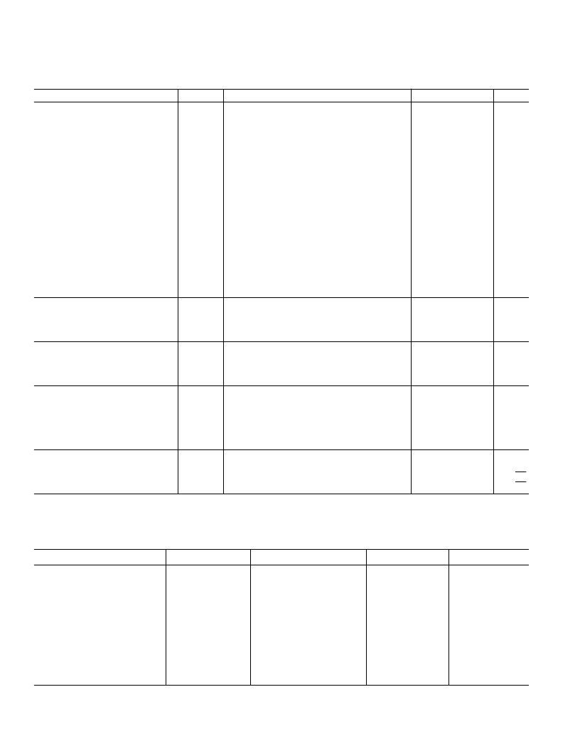
ELECTRICAL CHARACTERISTICS
Parameter
INPUT CHARACT ERIST ICS
Offset Voltage “OP184/284E” Grade
Symbol
Conditions
Min
T yp
Max
Units
V
OS
(Note 1)
–40
°
C
≤
T
A
≤
+125
°
C
100
200
175
375
150
300
250
500
300
500
50
+15
μ
V
μ
V
μ
V
μ
V
μ
V
μ
V
μ
V
μ
V
nA
nA
nA
V
dB
dB
V/mV
V/mV
μ
V/
°
C
pA/
°
C
Offset Voltage “284F” Grade
V
OS
–40
°
C
≤
T
A
≤
+125
°
C
Offset Voltage “484E” Grade
V
OS
–40
°
C
≤
T
A
≤
+125
°
C
Offset Voltage “484F” Grade
V
OS
–40
°
C
≤
T
A
≤
+125
°
C
Input Bias Current
I
B
80
–40
°
C
≤
T
A
≤
+125
°
C
–40
°
C
≤
T
A
≤
+125
°
C
Input Offset Current
Input Voltage Range
Common-Mode Rejection Ratio
Common-Mode Rejection Ratio
Large Signal Voltage Gain
I
OS
–15
86
80
150
75
CMRR
CMRR
A
VO
V
CM
= –14.0 V to +14.0 V, –40
°
C
≤
T
A
≤
+125
°
C
V
CM
= –15.0 V to +15.0 V
R
L
= 2 k
, –10 V
≤
V
O
≤
10 V
R
L
= 2 k
, –40
°
C
≤
T
A
≤
+125
°
C
90
1000
Offset Voltage Drift
Bias Current Drift
OUT PUT CHARACT ERIST ICS
Output Voltage High
Output Voltage Low
Output Current
POWER SUPPLY
Power Supply Rejection Ratio
Supply Current/Amplifier
Supply Current/Amplifier
DYNAMIC PERFORMANCE
Slew Rate
Full-Power Bandwidth
Settling T ime
Gain Bandwidth Product
Phase Margin
NOISE PERFORMANCE
Voltage Noise
Voltage Noise Density
Current Noise Density
“E” Grade
V
OS
/
T
I
B
/
T
0.2
150
2.00
V
OH
V
OL
I
OUT
I
L
= 1.0 mA
I
L
= 1.0 mA
+14.8
V
–14.875
V
±
10
mA
PSRR
I
SY
I
SY
V
S
=
±
2.0 V to
±
18 V, –40
°
C
≤
T
A
≤
+125
°
C
V
O
= 0 V, –40
°
C
≤
T
A
≤
+125
°
C
V
S
=
±
18 V, –40
°
C
≤
T
A
≤
+125
°
C
90
dB
mA
mA
1.75
2.0
SR
BW
p
t
S
GBP
o
R
L
= 2 k
1% Distortion, R
L
= 2 k
, V
O
= 29 V p-p
T o 0.01%, 10 V Step
2.4
4.0
35
4
4.25
50
V/
μ
s
kHz
μ
s
MHz
Degrees
e
n
p-p
e
n
i
n
0.1 Hz to 10 Hz
f = 1 kHz
0.3
3.9
0.4
μ
V p-p
nV/
√
Hz
pA/
√
Hz
NOT ES
1
Input Offset Voltage measurements are performed by automated test equipment approximately 0.5 seconds after application of power.
Specifications subject to change without notice.
WAFER TEST LIMTS
(@ V
S
= +5.0 V, V
CM
= 2.5 V, T
A
= +25
8
C unless otherwse noted)
(@ V
S
=
6
15.0 V, V
CM
= 0 V, T
A
= +25
8
C unless otherwse noted)
Parameter
Symbol
Conditions
Limit
Units
Offset Voltage OP284
Offset Voltage OP484
Input Bias Current
Input Offset Current
Input Voltage Range
Common-Mode Rejection Ratio
Power Supply Rejection Ratio
Large Signal Voltage Gain
Output Voltage High
Output Voltage Low
Supply Current/Amplifier
V
OS
V
OS
I
B
I
OS
V
CM
CMRR
PSRR
A
VO
V
OH
V
OL
I
SY
65
75
300
50
V– to V+
86
90
50
4.85
125
1.25
μ
V max
μ
V max
nA max
nA max
V min
dB min
dB min
V/mV min
V min
mV max
mA max
V
CM
= +1 V to +4 V
V
S
=
±
2 V to
±
18 V
R
L
= 2 k
I
L
= 1.0 mA
I
L
= 1.0 mA
V
O
= 0 V, R
L
=
∞
NOT E
Electrical tests and wafer probe to the limits shown. Due to variations in assembly methods and normal yield loss, yield after packaging is not guaranteed for standard
product dice. Consult factory to negotiate specifications based on dice lot qualifications through sample lot assembly and testing.
相关PDF资料 |
PDF描述 |
|---|---|
| OP490FY | Low Voltage Micropower Quad Operational Amplifier |
| OP490AY | Low Voltage Micropower Quad Operational Amplifier |
| OP490EY | Low Voltage Micropower Quad Operational Amplifier |
| OP490GP | Low Voltage Micropower Quad Operational Amplifier |
| OP490GS | Low Voltage Micropower Quad Operational Amplifier |
相关代理商/技术参数 |
参数描述 |
|---|---|
| OP4840002C | 制造商:Analog Devices 功能描述: |
| OP4840016SZR7 | 制造商:Analog Devices 功能描述: |
| OP484AM-EMX | 制造商:Analog Devices 功能描述:OP484AM-EMX - Bulk |
| OP484AY/QMLR | 制造商:Analog Devices 功能描述: |
发布紧急采购,3分钟左右您将得到回复。