- 您现在的位置:买卖IC网 > PDF目录6076 > OP496HRUZ-REEL (Analog Devices Inc)IC OPAMP QUAD R-R MCRPWR 14TSSOP PDF资料下载
参数资料
| 型号: | OP496HRUZ-REEL |
| 厂商: | Analog Devices Inc |
| 文件页数: | 4/19页 |
| 文件大小: | 0K |
| 描述: | IC OPAMP QUAD R-R MCRPWR 14TSSOP |
| 标准包装: | 1 |
| 放大器类型: | 通用 |
| 电路数: | 4 |
| 输出类型: | 满摆幅 |
| 转换速率: | 0.3 V/µs |
| 增益带宽积: | 450kHz |
| 电流 - 输入偏压: | 10nA |
| 电压 - 输入偏移: | 35µV |
| 电流 - 电源: | 60µA |
| 电流 - 输出 / 通道: | 4mA |
| 电压 - 电源,单路/双路(±): | 3 V ~ 12 V,±1.5 V ~ 6 V |
| 工作温度: | -40°C ~ 125°C |
| 安装类型: | 表面贴装 |
| 封装/外壳: | 14-TSSOP(0.173",4.40mm 宽) |
| 供应商设备封装: | 14-TSSOP |
| 包装: | 标准包装 |
| 产品目录页面: | 768 (CN2011-ZH PDF) |
| 其它名称: | OP496HRUZ-REELDKR |
OP196/OP296/OP496
REV.
–12–
APPLICATIONS INFORMATION
Functional Description
The OP196 family of operational amplifiers is comprised of single-
supply, micropower, rail-to-rail input and output amplifiers. Input
offset voltage (VOS) is only 300
V maximum, while the output
will deliver
±5 mA to a load. Supply current is only 50 A, while
bandwidth is over 450 kHz and slew rate is 0.3 V/
s. TPC 36 is
a simplified schematic of the OP196—it displays the novel cir-
cuit design techniques used to achieve this performance.
Input Overvoltage Protection
The OPx96 family of op amps uses a composite PNP/NPN
input stage. Transistor Q1 in Figure 36 has a collector-base
voltage of 0 V if +IN = VEE. If +IN then exceeds VEE, the junc-
tion will be forward biased and large diode currents will flow,
which may damage the device. The same situation applies to
+IN on the base of transistor Q5 being driven above VCC. There-
fore, the inverting and noninverting inputs must not be driven
above or below either supply rail unless the input current is
limited.
Figure 1 shows the input characteristics for the OPx96 family.
This photograph was generated with the power supply pins
connected to ground and a curve tracer’s collector output drive
connected to the input. As shown in the figure, when the input
voltage exceeds either supply by more than 0.6 V, internal
pn-junctions energize and permit current flow from the inputs
to the supplies. If the current is not limited, the amplifier may
be damaged. To prevent damage, the input current should be
limited to no more than 5 mA.
10
0%
100
90
8
6
4
2
0
–2
–4
–6
–8
–1.5
–1 –0.5
0
0.5
1
1.5
INPUT VOLTAGE – V
INPUT
CURRENT
–
mA
Figure 1. Input Overvoltage I-V Characteristics of the
OPx96 Family
Output Phase Reversal
Some other operational amplifiers designed for single-supply
operation exhibit an output voltage phase reversal when their
inputs are driven beyond their useful common-mode range.
Typically for single-supply bipolar op amps, the negative supply
determines the lower limit of their common-mode range. With
these common-mode limited devices, external clamping diodes
are required to prevent input signal excursions from exceeding
the device’s negative supply rail (i.e., GND) and triggering
output phase reversal.
The OPx96 family of op amps is free from output phase reversal
effects due to its novel input structure. Figure 2 illustrates the
performance of the OPx96 op amps when the input is driven
beyond the supply rails. As previously mentioned, amplifier
input current must be limited if the inputs are driven beyond
the supply rails. In the circuit of Figure 2, the source ampli-
tude is
± 15 V, while the supply voltage is only ± 5 V. In this
case, a 2 k
source resistor limits the input current to 5 mA.
10
0%
100
90
VS = 5V
AV = 1
5V
1ms
5V
0
VIN
VOUT
VOLTAGE
–
5
V/DI
V
TIME – 1ns/DIV
Figure 2. Output Voltage Phase Reversal Behavior
Input Offset Voltage Nulling
The OP196 provides two offset adjust terminals that can be
used to null the amplifier’s internal VOS. In general, operational
amplifier terminals should never be used to adjust system offset
voltages. A 100 k
potentiometer, connected as shown in Fig-
ure 3, is recommended to null the OP196’s offset voltage. Offset
nulling does not adversely affect TCVOS performance, providing
that the trimming potentiometer temperature coefficient does
not exceed
±100 ppm/°C.
6
7
2
3
V–
V+
OP196
100k
4
1
5
Figure 3. Offset Nulling Circuit
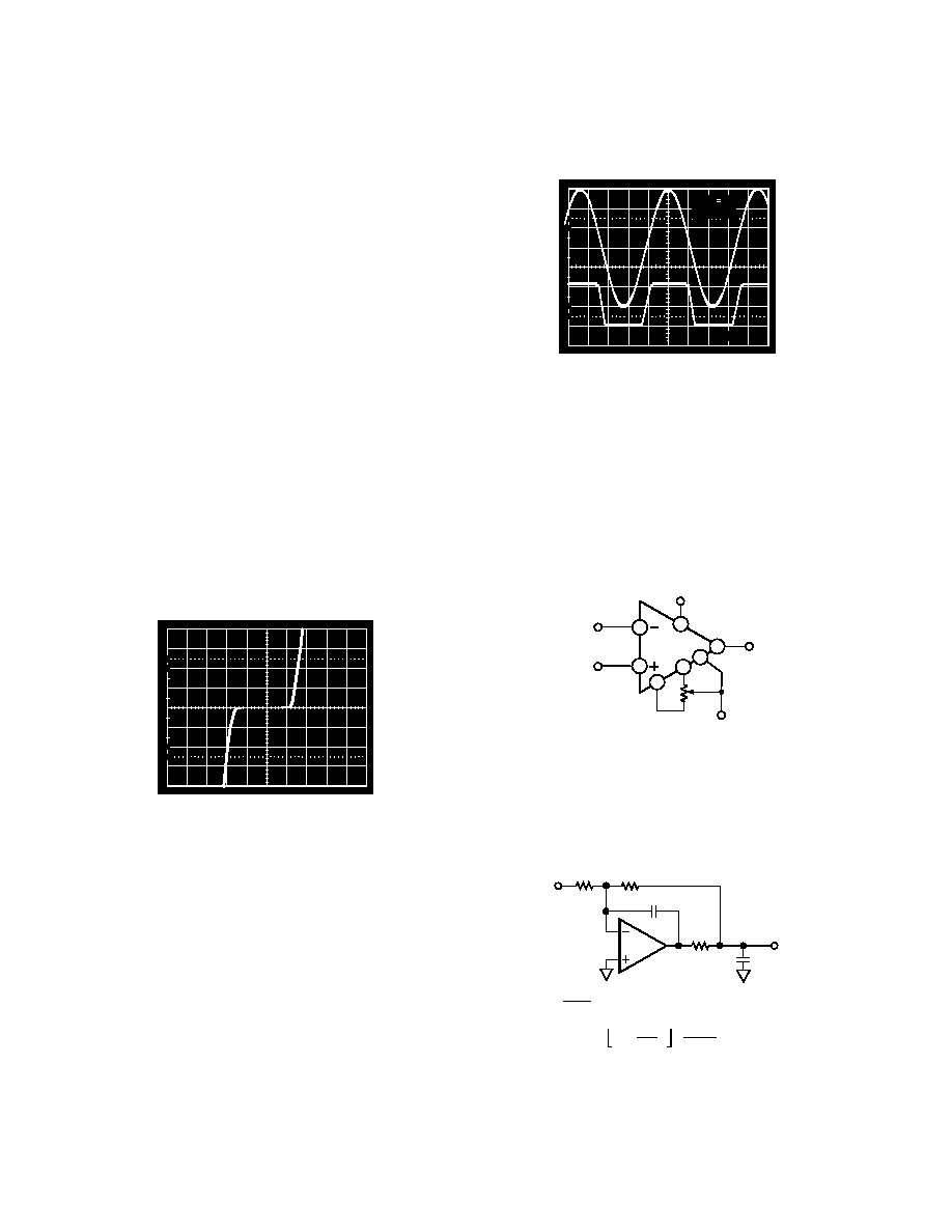
Driving Capacitive Loads
OP196 family amplifiers are unconditionally stable with capaci-
tive loads less than 170 pF. When driving large capacitive loads
in unity-gain configurations, an in-the-loop compensation
technique is recommended, as illustrated in Figure 4.
OP296
CF
VIN
RG
RF
RX
CL
VOUT
RX =
WHERE RO = OPEN-LOOP OUTPUT RESISTANCE
RO RG
RF
CF = I + (
) (
) C
L RO
I
|ACL|
RF + RG
RF
Figure 4. In-the-Loop Compensation Technique for
Driving Capacitive Loads
E
相关PDF资料 |
PDF描述 |
|---|---|
| 68046-237LF | CONN RCPT 74POS .100" DBL SMD |
| 929834-01-24-RK | CONN HEADER 24POS SNGL .100 STR |
| SSW-150-02-S-D | CONN RCPT .100" 100POS DUAL GOLD |
| TSW-120-08-T-S-RA | CONN HEADER 20POS .100" SNGL R/A |
| 929500-01-11-RK | CONN HEADER .100 SNGL R/A 11POS |
相关代理商/技术参数 |
参数描述 |
|---|---|
| OP497 | 制造商:AD 制造商全称:Analog Devices 功能描述:Precision Picoampere Input Current Quad Operational Amplifier |
| OP-497 | 制造商:AD 制造商全称:Analog Devices 功能描述:PRECISION PICOAMPERE INPUT CURRENT QUAD OPERATIONAL AMPLIFIER |
| OP4970027SR | 制造商:Analog Devices 功能描述: |
| OP497AY | 制造商:AD 制造商全称:Analog Devices 功能描述:Precision Picoampere Input Current Quad Operational Amplifier |
| OP-497AY | 制造商:AD 制造商全称:Analog Devices 功能描述:PRECISION PICOAMPERE INPUT CURRENT QUAD OPERATIONAL AMPLIFIER |
发布紧急采购,3分钟左右您将得到回复。