参数资料
| 型号: | OPA170AIDBVR |
| 厂商: | Texas Instruments |
| 文件页数: | 6/34页 |
| 文件大小: | 0K |
| 描述: | IC OPAMP GP RR 1.2MHZ SOT23-5 |
| 标准包装: | 3,000 |
| 放大器类型: | 通用 |
| 电路数: | 1 |
| 输出类型: | 满摆幅 |
| 转换速率: | 0.4 V/µs |
| 增益带宽积: | 1.2MHz |
| 电流 - 输入偏压: | 8pA |
| 电压 - 输入偏移: | 250µV |
| 电流 - 电源: | 110µA |
| 电流 - 输出 / 通道: | 20mA |
| 电压 - 电源,单路/双路(±): | 2.7 V ~ 36 V,±1.35 V ~ 18 V |
| 工作温度: | -40°C ~ 125°C |
| 安装类型: | 表面贴装 |
| 封装/外壳: | SC-74A,SOT-753 |
| 供应商设备封装: | SOT-23-5 |
| 包装: | 带卷 (TR) |
第1页第2页第3页第4页第5页当前第6页第7页第8页第9页第10页第11页第12页第13页第14页第15页第16页第17页第18页第19页第20页第21页第22页第23页第24页第25页第26页第27页第28页第29页第30页第31页第32页第33页第34页
W
OPA170
R =
I
10kW
R
OUT
C
L
R
F
=10kW
+18V
-18V
G=
1
-
W
+18V
-18V
R
OUT
C
L
OPA170
R
L
G=+1
5kW
OPA170
10mAmax
V+
V
IN
V
OUT
I
OVERLOAD
SBOS557B – AUGUST 2011 – REVISED SEPTEMBER 2012
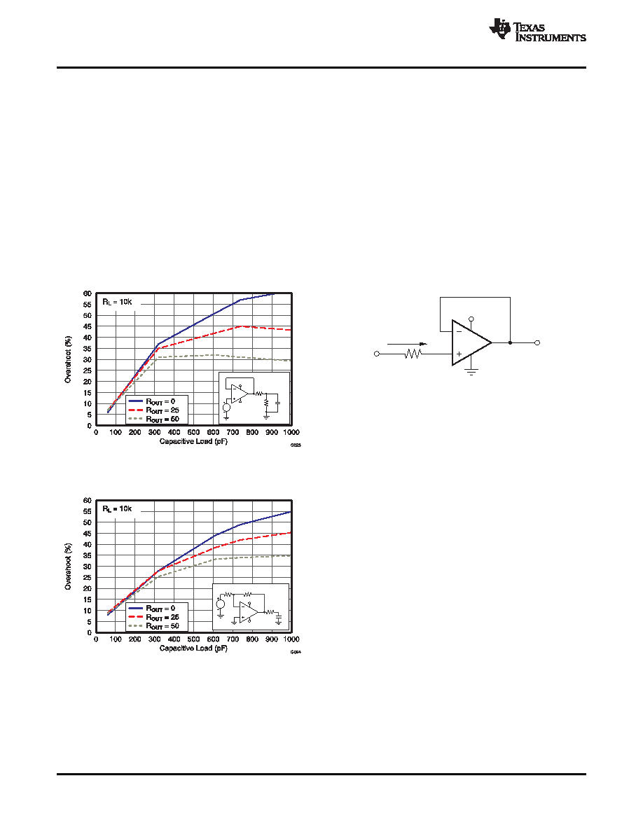
CAPACITIVE LOAD AND STABILITY
or even the output pin. Each of these different pin
The dynamic characteristics of the OPAx170 have
functions have electrical stress limits determined by
been optimized for common operating conditions. The
the
voltage
breakdown
characteristics
of
the
combination
of
low
closed-loop
gain
and
high
particular semiconductor fabrication process and
capacitive loads decreases the phase margin of the
specific circuits connected to the pin. Additionally,
amplifier and can lead to gain peaking or oscillations.
internal electrostatic discharge (ESD) protection is
As a result, heavier capacitive loads must be isolated
built
into
these
circuits
to
protect
them
from
from the output. The simplest way to achieve this
accidental ESD events both before and during
isolation is to add a small resistor (for example, ROUT
product assembly.
equal to 50
Ω) in series with the output. Figure 38 and
These ESD protection diodes also provide in-circuit,
Figure 39 illustrate graphs of small-signal overshoot
input overdrive protection, as long as the current is
versus capacitive load for several values of ROUT.
limited to 10mA as stated in the Absolute Maximum
Also, refer to Applications Bulletin AB-028, Feedback
Plots Define Op Amp AC Performance (literature
may be added to the driven input to limit the input
number SBOA015, available for download from the TI
current. The added resistor contributes thermal noise
website), for details of analysis techniques and
at the amplifier input and its value should be kept to a
application circuits.
minimum in noise-sensitive applications.
Figure 40. Input Current Protection
An ESD event produces a short duration, high-
voltage pulse that is transformed into a short
duration, high-current pulse as it discharges through
a semiconductor device. The ESD protection circuits
Figure 38. Small-Signal Overshoot versus
are designed to provide a current path around the
Capacitive Load (100mV Output Step, G = +1)
operational amplifier core to prevent it from being
damaged. The energy absorbed by the protection
circuitry is then dissipated as heat.
When the operational amplifier connects into a circuit,
the ESD protection components are intended to
remain inactive and not become involved in the
application circuit operation. However, circumstances
may arise where an applied voltage exceeds the
operating voltage range of a given pin. Should this
condition occur, there is a risk that some of the
internal ESD protection circuits may be biased on,
and conduct current. Any such current flow occurs
through ESD cells and rarely involves the absorption
device.
If there is an uncertainty about the ability of the
supply to absorb this current, external zener diodes
Figure 39. Small-Signal Overshoot versus
may be added to the supply pins. The zener voltage
Capacitive Load (100mV Output Step, G = –1)
must be selected such that the diode does not turn
on during normal operation. However, its zener
voltage should be low enough so that the zener diode
ELECTRICAL OVERSTRESS
conducts if the supply pin begins to rise above the
safe operating supply voltage level.
Designers often ask questions about the capability of
an
operational
amplifier
to
withstand
electrical
overstress. These questions tend to focus on the
device inputs, but may involve the supply voltage pins
14
Copyright 2011–2012, Texas Instruments Incorporated
相关PDF资料 |
PDF描述 |
|---|---|
| 170M6467 | FUSE 1400A 690V 3BKN/50 AR UC |
| 10075024-G01-09ULF | CONN HEADER 18POS VERT 2MM GOLD |
| SM6S10AHE3/2D | TVS 6W 10V 5% SMD DO-218AB |
| 170M6469 | FUSE 1600A 690V 3BKN/65 AR UC |
| 170M6468 | FUSE 1500A 690V 3BKN/50 AR UC |
相关代理商/技术参数 |
参数描述 |
|---|---|
| OPA170AIDBVT | 功能描述:运算放大器 - 运放 36V,MICROPOWER,RRO GEN PURP OP AMP RoHS:否 制造商:STMicroelectronics 通道数量:4 共模抑制比(最小值):63 dB 输入补偿电压:1 mV 输入偏流(最大值):10 pA 工作电源电压:2.7 V to 5.5 V 安装风格:SMD/SMT 封装 / 箱体:QFN-16 转换速度:0.89 V/us 关闭:No 输出电流:55 mA 最大工作温度:+ 125 C 封装:Reel |
| OPA170AIDR | 功能描述:运算放大器 - 运放 36V,MICROPOWER,RRO GEN PURP OP AMP RoHS:否 制造商:STMicroelectronics 通道数量:4 共模抑制比(最小值):63 dB 输入补偿电压:1 mV 输入偏流(最大值):10 pA 工作电源电压:2.7 V to 5.5 V 安装风格:SMD/SMT 封装 / 箱体:QFN-16 转换速度:0.89 V/us 关闭:No 输出电流:55 mA 最大工作温度:+ 125 C 封装:Reel |
| OPA170AIDRLR | 制造商:Texas Instruments 功能描述:OP Amp Single GP R-R O/P 制造商:Texas Instruments 功能描述:OP Amp Single GP R-R O/P ±18V/36V 5-Pin SOT T/R 制造商:Texas Instruments 功能描述:IC OPAMP GP RRO 1.2MHZ SOT553-5 制造商:Texas Instruments 功能描述:36V,microPower,RRO, Gen Purp Op Amp |
| OPA170AIDRLT | 功能描述:运算放大器 - 运放 36V,microPower,RRO, Gen Purp Op Amp RoHS:否 制造商:STMicroelectronics 通道数量:4 共模抑制比(最小值):63 dB 输入补偿电压:1 mV 输入偏流(最大值):10 pA 工作电源电压:2.7 V to 5.5 V 安装风格:SMD/SMT 封装 / 箱体:QFN-16 转换速度:0.89 V/us 关闭:No 输出电流:55 mA 最大工作温度:+ 125 C 封装:Reel |
| OPA170AQDBVRQ1 | 功能描述:IC OP AMP GP RR 1.2MHZ 5-SOT-23 制造商:texas instruments 系列:汽车级,AEC-Q100 包装:剪切带(CT) 零件状态:在售 放大器类型:通用 电路数:1 输出类型:满摆幅 压摆率:0.4 V/μs 增益带宽积:1.2MHz 电流 - 输入偏置:8pA 电压 - 输入失调:250μV 电流 - 电源:110μA 电流 - 输出/通道:17mA 电压 - 电源,单/双(±):2.7 V ~ 36 V,±1.35 V ~ 18 V 工作温度:-40°C ~ 125°C 安装类型:表面贴装 封装/外壳:SC-74A,SOT-753 供应商器件封装:SOT-23-5 标准包装:1 |
发布紧急采购,3分钟左右您将得到回复。