参数资料
| 型号: | OPA567AIRHGT |
| 厂商: | Texas Instruments |
| 文件页数: | 7/26页 |
| 文件大小: | 0K |
| 描述: | IC OPAMP GP R-R 1.2MHZ 12VQFN |
| 标准包装: | 1 |
| 放大器类型: | 通用 |
| 电路数: | 1 |
| 输出类型: | 满摆幅 |
| 转换速率: | 1.2 V/µs |
| 增益带宽积: | 1.2MHz |
| 电流 - 输入偏压: | 1pA |
| 电压 - 输入偏移: | 500µV |
| 电流 - 电源: | 9mA |
| 电流 - 输出 / 通道: | 2.4A |
| 电压 - 电源,单路/双路(±): | 2.5 V ~ 5.5 V,±1.25 V ~ 2.75 V |
| 工作温度: | -40°C ~ 85°C |
| 安装类型: | 表面贴装 |
| 封装/外壳: | 12-VQFN 裸露焊盘 |
| 供应商设备封装: | 12-VQFN-EP(5x5) |
| 包装: | 标准包装 |
| 产品目录页面: | 854 (CN2011-ZH PDF) |
| 其它名称: | 296-18697-6 |
OPA567
SBOS287A
15
www.ti.com
ENSURING MICROCONTROLLER COMPATIBILITY
Not all microcontrollers output the same logic state after
power-up or reset. 8051-type microcontrollers, for example,
output logic High levels on their ports while other models
power up with logic Low levels after reset.
In configuration (a) shown in Figure 4, the enable/disable
signal is applied on the cathode side of the photodiode within
the optocoupler. A logic High level causes the OPA567 to be
enabled, and a logic Low level disables the OPA567. In
configuration (b) of Figure 4, with the logic signal applied on
the anode side, a high level disables the OPA567 and a low
level enables the op amp.
RAIL-TO-RAIL OUTPUT RANGE
The OPA567 has a class AB output stage with common
source transistors that are used to achieve rail-to-rail output
swing. It was designed to be able to swing closer to the rail
than other existing linear amplifiers, even with high output
current levels. A quick way to estimate the output swing with
various output current requirements is by using the equation:
VSWING [typical] = 0.1 IO
Plots of the Output Swing vs Output Current, Supply Voltage,
and Temperature are provided in the Typical Characteristics
section.
RAIL-TO-RAIL INPUT RANGE
The input common-mode voltage range of the OPA567
extends 100mV beyond the supply rails. This is achieved by
a complementary input stage with an N-channel input differ-
ential pair in parallel with a P-channel differential pair. The
N-channel input pair is active for input voltages close to the
positive rail while the P-channel input pair is active for input
voltages close to the negative rail. The transition point is
typically at (V+) – 1.3V, and there is a small transition region
around the switching point where both transistors are on. It
is important to note that the two input pairs can have offsets
of different signs and magnitudes. Therefore, as the transi-
tion point is crossed, the offset of the amplifier changes. This
offset shift accounts for the reduced common-mode rejection
ratio over the full input common-mode range.
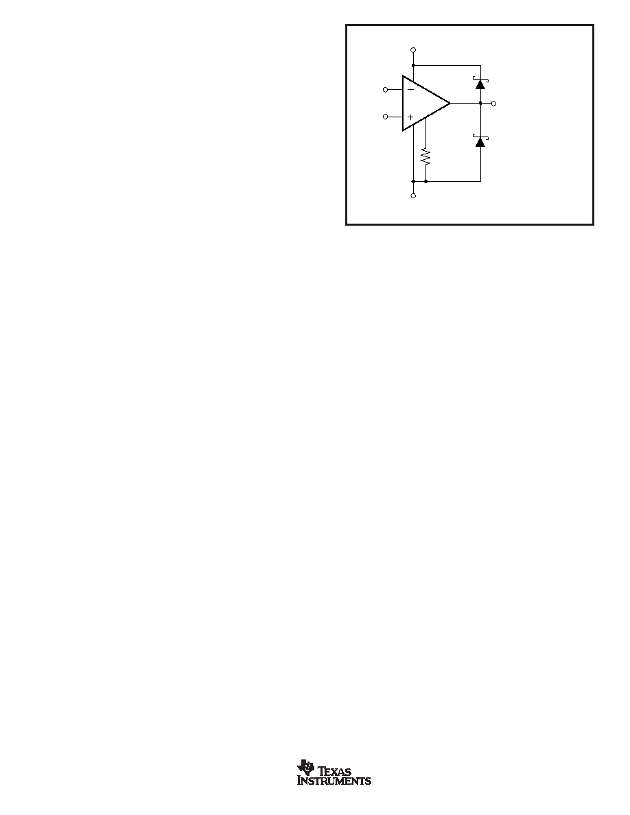
OUTPUT PROTECTION
Reactive and EMF-generating loads can return load current
to the amplifier, causing the output voltage to exceed the
power-supply voltage. This damaging condition can be
avoided with clamp diodes from the output terminal to the
power supplies, as shown in Figure 5. Schottky rectifier
diodes with a 3A or greater continuous rating are recom-
mended.
THERMAL FLAG PIN
The OPA567 has thermal sensing circuitry that provides a
warning signal when the die temperature exceeds safe limits.
Unless the TFLAG pin is connected to the Enable pin, when
this flag is triggered, the part continues to operate even
though the junction temperature exceeds 150
°C. This default
operation allows maximum usable operation in very harsh
conditions but degrades reliability. The TFLAG pin can be used
to provide for orderly system shutdown before failure occurs.
It can be also used to evaluate the thermal environment to
determine need for and appropriate design of a shutdown
mechanism.
The thermal flag output signal is from a CMOS logic gate that
switches from V+ to V– to indicate that the amplifier is in
thermal limit. This flag output pin can source and sink up to
25
A. The T
FLAG pin is HIGH during normal operation. Power
dissipated in the amplifier will cause the junction temperature
to rise. When the junction temperature exceeds 150
°C, the
TFLAG pin will go Low, and remain Low until the amplifier has
cooled to 130
°C. Despite this hysteresis, with a method of
orderly shutdown, the TFLAG pin can cycle on and off, de-
pending on load and signal conditions. This limits the dissi-
pation of the amplifier but may have an undesirable effect on
the load.
It is possible to connect the TFLAG pin directly to the Enable
pin for automatic shutdown protection. When both thermal
shutdown and the amplifier enable/disable functions are
desired, the externally generated control signal and the TFLAG
pin outputs should be combined with an AND gate; see
Figure 6. The temperature protection was designed to pro-
tect against overload conditions. It was not intended to
replace proper heatsinking. Continuously running the OPA567
in and out of thermal shutdown will degrade reliability.
FIGURE 5. Output Protection Diode.
OPA567
Output Protection Diode
I
SET
R
SET
V
O
+V
1, 12
6
8
9
4, 5
–In
+In
2, 3
–V
相关PDF资料 |
PDF描述 |
|---|---|
| RMCF2010FT36R5 | RES 36.5 OHM 1% 3/4W 2010 SMD |
| RMCF2010FT33K2 | RES 33.2K OHM 1% 3/4W 2010 SMD |
| ESQT-104-03-F-D-310 | CONN SOCKET 8 POS DUAL ROW |
| RMCF2010FT2K49 | RES 2.49K OHM 1% 3/4W 2010 SMD |
| PPTC322LJBN-RC | CONN FEMALE 64POS DL .1" R/A TIN |
相关代理商/技术参数 |
参数描述 |
|---|---|
| OPA567AIRHGT | 制造商:Texas Instruments 功能描述:IC OP-AMP GP R-R 1.2MHZ 12VQFN |
| OPA567AIRHGTG4 | 功能描述:运算放大器 - 运放 Rail-to-Rail I/O 2A Power Amplifier RoHS:否 制造商:STMicroelectronics 通道数量:4 共模抑制比(最小值):63 dB 输入补偿电压:1 mV 输入偏流(最大值):10 pA 工作电源电压:2.7 V to 5.5 V 安装风格:SMD/SMT 封装 / 箱体:QFN-16 转换速度:0.89 V/us 关闭:No 输出电流:55 mA 最大工作温度:+ 125 C 封装:Reel |
| OPA569 | 制造商:未知厂家 制造商全称:未知厂家 功能描述:Power Op Amp. Output Signal Swings Within 200mV of Rails at 2A Output Current |
| OPA569AIDWP | 功能描述:运算放大器 - 运放 2A Pwr Op Amp Rail-To-Rail I/O RoHS:否 制造商:STMicroelectronics 通道数量:4 共模抑制比(最小值):63 dB 输入补偿电压:1 mV 输入偏流(最大值):10 pA 工作电源电压:2.7 V to 5.5 V 安装风格:SMD/SMT 封装 / 箱体:QFN-16 转换速度:0.89 V/us 关闭:No 输出电流:55 mA 最大工作温度:+ 125 C 封装:Reel |
| OPA569AIDWPG4 | 功能描述:运算放大器 - 运放 2A Pwr Op Amp Rail-To-Rail I/O RoHS:否 制造商:STMicroelectronics 通道数量:4 共模抑制比(最小值):63 dB 输入补偿电压:1 mV 输入偏流(最大值):10 pA 工作电源电压:2.7 V to 5.5 V 安装风格:SMD/SMT 封装 / 箱体:QFN-16 转换速度:0.89 V/us 关闭:No 输出电流:55 mA 最大工作温度:+ 125 C 封装:Reel |
发布紧急采购,3分钟左右您将得到回复。