- 您现在的位置:买卖IC网 > Datasheet目录62 > OPB815W (TT Electronics/Optek Technology)SENS OPTO SLOT 9.53MM TRANS C-MT Datasheet资料下载
参数资料
| 型号: | OPB815W |
| 厂商: | TT Electronics/Optek Technology |
| 文件页数: | 2/3页 |
| 文件大小: | 160K |
| 描述: | SENS OPTO SLOT 9.53MM TRANS C-MT |
| 标准包装: | 1 |
| 检测距离: | 0.375" (9.53mm) |
| 检测方法: | 可传导的 |
| 输出配置: | 光电晶体管 |
| 电流 - DC 正向(If): | 50mA |
| 电压 - 集电极发射极击穿(最大): | 30V |
| 安装类型: | 底座安装 |
| 封装/外壳: | 模块,预接线 |
| 包装: | 散装 |
| 类型: | 无放大 |
| 工作温度: | -40°C ~ 80°C |
OPTEK Technology Inc. 1645 Wallace Drive, Carrollton, Texas 75006
Phone: (972) 323-2200 or (800) 341-4747 FAX: (972) 323-2396 sensors@optekinc.com www.optekinc.com
Issue A.5 01/14
Page 2 of 3
OPTEK reserves the right to make changes at any time in order to improve design and to supply the best product possible.
Deep Gap Slotted Switch with Wire and
Connector Options
OPB815L, OPB815WZ Series
Electrical Characteristics (T
A
= 25癈 unless otherwise noted)
SYMBOL
PARAMETER
MIN TYP MAX UNITS
TEST CONDITIONS
Input Infrared LED (see OP240 for additional information)
V
F
Forward Voltage
- - 1.7 V I
F
= 20 mA
I
R
Reverse Current
- - 100 礎 V
R
= 2 V
Output Phototransistor (see OP550 for additional information)
V
(BR)CEO
Collector-Emitter Breakdown Voltage 30 - - V I
C
= 1 mA
V
(BR)ECO
Emitter-Collector Breakdown Voltage 5 - - v I
E
= 100 礎
I
CEO
Collector-Emitter Dark Current
- - 100 nA V
CE
= 10 V, I
F
= 0, E
E
= 0
Coupled
V
CE(SAT)
Collector-Emitter Saturation Voltage - - 0.4 V I
C
= 500 礎, I
F
= 20 mA
I
C(ON)
On-State Collector Current
3.5 - 16 mA V
CE
= 10 V, I
F
= 20 mA
Absolute Maximum Ratings (T
A
=25癈 unless otherwise noted)
Storage & Operating Temperature Range
-40?C to +80?C
Lead Soldering Temperature [1/16 inch (1.6mm) from the case for 5 sec. with soldering iron]
260?C
Input Infrared LED
Continuous Forward Current
50 mA
Reverse Voltage
2 V
Power Dissipation
(2)
100 mW
Output Phototransistor
Collector-Emitter Voltage
30 V
Emitter-Collector Voltage
5 V
Power Dissipation
(2)
100 mW
Notes:
(1) All wires are 26 AWG stranded, UL rated.
(2) Derate linearly 1.67mW/癈 above 25?C.
(3) Methanol or isopropanol are recommended as cleaning agents.
The plastic housing is soluble in chlorinated hydrocarbons and
keytones.
(4) All parameters tested using pulse techniques.
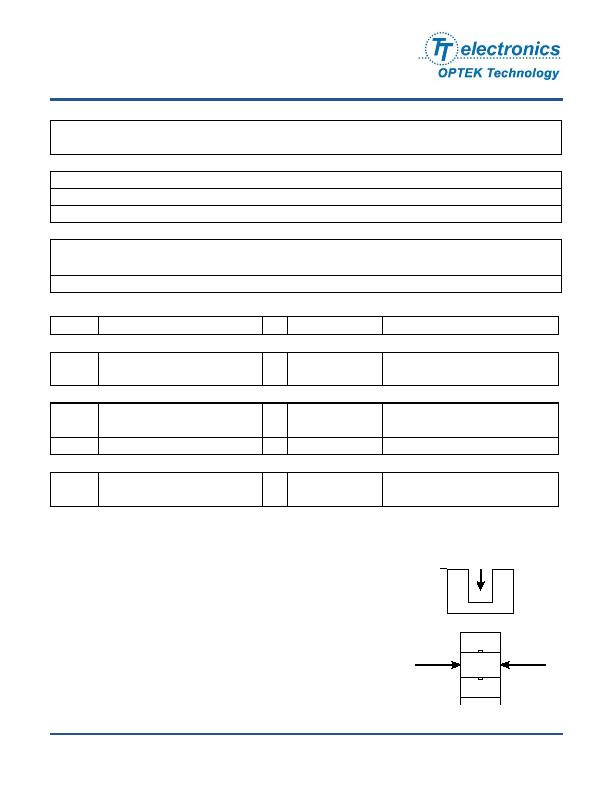
Emitter
Sensor
Left to Right
Right to Left
0
Width
Top to Bottom
0
Test Diagram
相关PDF资料 |
PDF描述 |
|---|---|
| OPB821S5Z | SENS OPTO SLOT 2.03MM TRANS C-MT |
| OPB821TXV | SENS OPTO SLOT 2.03MM TRANS C-MT |
| OPB825B | SENS OPTO SLOT 4.06MM TRANS THRU |
| OPB826SD | SENS OPTO SLOT 2.29MM 2 NPN THRU |
| OPB829B | SENS OPTO SLOT 3.18MM TRANS C-MT |
相关代理商/技术参数 |
参数描述 |
|---|---|
| OPB-815W | 制造商:TT Electronics / OPTEK Technology 功能描述: |
| OPB815W_06 | 制造商:OPTEK 制造商全称:OPTEK 功能描述:DEEP GAP SLOTTED OPTICAL SWITCH |
| OPB815WZ | 功能描述:光学开关(透射型,光电晶体管输出) .375in Slot Ir RoHS:否 制造商:Omron Electronics 输出设备:Phototransistor 槽宽:3.4 mm 光圈宽度:0.5 mm 集电极—发射极最大电压 VCEO:30 V 最大集电极电流:20 mA 正向电流: 安装风格:Through Hole 最大工作温度:+ 85 C 最小工作温度:- 25 C 封装: |
| OPB815W-Z | 制造商:TT Electronics / OPTEK Technology 功能描述:OPTO SWITCH SLOTTED |
| OPB816 | 功能描述:光学开关(透射型,光电晶体管输出) Slotted Opt Switch RoHS:否 制造商:Omron Electronics 输出设备:Phototransistor 槽宽:3.4 mm 光圈宽度:0.5 mm 集电极—发射极最大电压 VCEO:30 V 最大集电极电流:20 mA 正向电流: 安装风格:Through Hole 最大工作温度:+ 85 C 最小工作温度:- 25 C 封装: |
发布紧急采购,3分钟左右您将得到回复。