- 您现在的位置:买卖IC网 > PDF目录224647 > OR2T08A-6BC160I (Electronic Theatre Controls, Inc.) Field-Programmable Gate Arrays PDF资料下载
参数资料
| 型号: | OR2T08A-6BC160I |
| 厂商: | Electronic Theatre Controls, Inc. |
| 元件分类: | FPGA |
| 英文描述: | Field-Programmable Gate Arrays |
| 中文描述: | 现场可编程门阵列 |
| 文件页数: | 58/192页 |
| 文件大小: | 3148K |
| 代理商: | OR2T08A-6BC160I |
第1页第2页第3页第4页第5页第6页第7页第8页第9页第10页第11页第12页第13页第14页第15页第16页第17页第18页第19页第20页第21页第22页第23页第24页第25页第26页第27页第28页第29页第30页第31页第32页第33页第34页第35页第36页第37页第38页第39页第40页第41页第42页第43页第44页第45页第46页第47页第48页第49页第50页第51页第52页第53页第54页第55页第56页第57页当前第58页第59页第60页第61页第62页第63页第64页第65页第66页第67页第68页第69页第70页第71页第72页第73页第74页第75页第76页第77页第78页第79页第80页第81页第82页第83页第84页第85页第86页第87页第88页第89页第90页第91页第92页第93页第94页第95页第96页第97页第98页第99页第100页第101页第102页第103页第104页第105页第106页第107页第108页第109页第110页第111页第112页第113页第114页第115页第116页第117页第118页第119页第120页第121页第122页第123页第124页第125页第126页第127页第128页第129页第130页第131页第132页第133页第134页第135页第136页第137页第138页第139页第140页第141页第142页第143页第144页第145页第146页第147页第148页第149页第150页第151页第152页第153页第154页第155页第156页第157页第158页第159页第160页第161页第162页第163页第164页第165页第166页第167页第168页第169页第170页第171页第172页第173页第174页第175页第176页第177页第178页第179页第180页第181页第182页第183页第184页第185页第186页第187页第188页第189页第190页第191页第192页
Data Sheet
ORCA Series 2 FPGAs
June 1999
150
Lucent Technologies Inc.
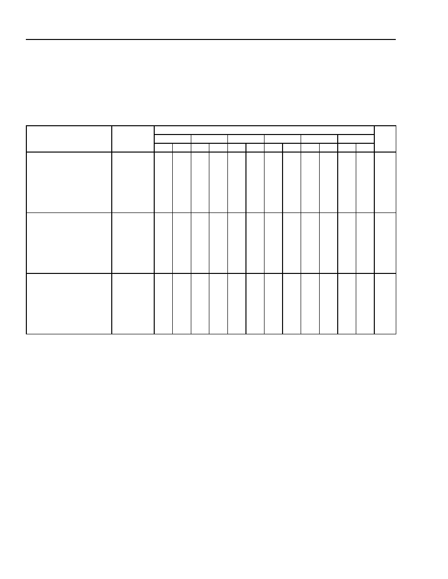
Timing Characteristics (continued)
Notes:
The pin-to-pin timing information from
ORCA Foundry version 9.2 and later is more accurate than this table. For earlier versions of ORCA
Foundry, the pin-to-pin timing parameters in this table should be used instead of results reported by
ORCA Foundry.
This clock delay is for a fully routed clock tree that uses the primary clock network. It includes both the input buffer delay, the clock routing to
the PFU CLK input, the clock
→Q of the FF, and the delay through the output buffer. The delay will be reduced if any of the clock branches are
not used. The given timing requires that the input clock pin be located at one of the four center PICs on any side of the device and that the
direct FF
→I/O routing be used.
If the clock pin is not located at one of the four center PICs, this delay must be increased by up to the following amounts:
OR2C/2T04A = 1.5%, OR2C/2T06A = 2.0%, OR2C/2T08A = 3.1%, OR2C/2T10A = 3.9%, OR2C/2T12A = 4.9%, OR2C/2T15A = 5.7%,
OR2C/2T26A = 8.1%, OR2C/2T40A = 12.5%.
Speed grades of -5, -6, and -7 are for OR2TxxA devices only.
Table 43A. OR2CxxA and OR2TxxA OR2CxxA/OR2TxxA Global Clock to Output Delay (Pin-to-Pin)—Output
on Same Side of the Device as the Clock Pin
OR2CxxA Commercial: VDD = 5.0 V ± 5%, 0 °C
≤ TA ≤ 70 °C; Industrial: VDD = 5.0 V ± 10%, –40 °C ≤ TA ≤ +85 °C; CL = 50 pF.
OR2TxxA Commercial: VDD = 3.0 V to 3.6 V, 0 °C
≤ TA ≤ 70 °C; Industrial: VDD = 3.0 V to 3.6 V, –40 °C ≤ TA ≤ +85 °C; CL =
50 pF.
Description
(TJ = 85 °C, VDD = min)
Device
Speed
Unit
-2
-3
-4
-5
-6
-7
Min
Max
Min
Max
Min
Max
Min
Max
Min
Max
Min
Max
CLK Input Pin
→ OUTPUT Pin
(Fast)
OR2C/2T04A
OR2C/2T06A
OR2C/2T08A
OR2C/2T10A
OR2C/2T12A
OR2C/2T15A
OR2C/2T26A
OR2C/2T40A
—
11.7
11.8
11.9
12.0
12.1
12.2
12.3
12.7
—
10.3
10.4
10.5
10.6
10.7
10.8
11.0
11.4
—
9.8
9.9
10.0
10.1
10.2
10.3
10.5
10.8
—
8.6
8.7
8.8
8.9
9.0
9.1
9.2
9.5
—
8.3
8.4
8.6
—
6.7
6.9
7.0
ns
CLK Input Pin
→ OUTPUT Pin
(Slewlim)
OR2C/2T04A
OR2C/2T06A
OR2C/2T08A
OR2C/2T10A
OR2C/2T12A
OR2C/2T15A
OR2C/2T26A
OR2C/2T40A
—
13.9
14.0
14.1
14.2
14.3
14.4
14.5
14.9
—
12.5
12.6
12.7
12.8
12.9
13.0
13.2
13.6
—
11.7
11.8
11.9
12.0
12.1
12.2
12.3
12.6
—
10.0
10.1
10.2
10.3
10.4
10.5
10.6
10.9
—
9.5
9.6
9.8
—
7.4
7.5
7.7
ns
CLK Input Pin
→ OUTPUT Pin
(Sinklim)
OR2C/2T04A
OR2C/2T06A
OR2C/2T08A
OR2C/2T10A
OR2C/2T12A
OR2C/2T15A
OR2C/2T26A
OR2C/2T40A
—
15.7
15.8
15.9
16.0
16.1
16.2
16.3
16.7
—
14.7
14.8
14.9
15.0
15.1
15.2
15.3
15.7
—
13.7
13.8
13.9
14.0
14.1
14.2
14.3
14.6
—
13.1
13.2
13.3
13.4
13.5
13.6
13.7
14.0
—
12.1
12.2
12.4
—
10.0
10.7
10.9
ns
相关PDF资料 |
PDF描述 |
|---|---|
| OR2T08A-6BC208 | Field-Programmable Gate Arrays |
| OR2T08A-6BC208I | Field-Programmable Gate Arrays |
| OR2T08A-6BC240 | Field-Programmable Gate Arrays |
| OR2T08A-6BC240I | Field-Programmable Gate Arrays |
| OR2T08A-6BC256 | Field-Programmable Gate Arrays |
相关代理商/技术参数 |
参数描述 |
|---|---|
| OR2T10A4BA256-DB | 功能描述:FPGA - 现场可编程门阵列 Use ECP/EC or XP RoHS:否 制造商:Altera Corporation 系列:Cyclone V E 栅极数量: 逻辑块数量:943 内嵌式块RAM - EBR:1956 kbit 输入/输出端数量:128 最大工作频率:800 MHz 工作电源电压:1.1 V 最大工作温度:+ 70 C 安装风格:SMD/SMT 封装 / 箱体:FBGA-256 |
| OR2T10A4BA256I-DB | 功能描述:FPGA - 现场可编程门阵列 1024 LUT 244 I/O RoHS:否 制造商:Altera Corporation 系列:Cyclone V E 栅极数量: 逻辑块数量:943 内嵌式块RAM - EBR:1956 kbit 输入/输出端数量:128 最大工作频率:800 MHz 工作电源电压:1.1 V 最大工作温度:+ 70 C 安装风格:SMD/SMT 封装 / 箱体:FBGA-256 |
| OR2T10A4J160-DB | 功能描述:FPGA - 现场可编程门阵列 1024 LUT 244 I/O RoHS:否 制造商:Altera Corporation 系列:Cyclone V E 栅极数量: 逻辑块数量:943 内嵌式块RAM - EBR:1956 kbit 输入/输出端数量:128 最大工作频率:800 MHz 工作电源电压:1.1 V 最大工作温度:+ 70 C 安装风格:SMD/SMT 封装 / 箱体:FBGA-256 |
| OR2T10A4J160I-DB | 功能描述:FPGA - 现场可编程门阵列 1024 LUT 244 I/O RoHS:否 制造商:Altera Corporation 系列:Cyclone V E 栅极数量: 逻辑块数量:943 内嵌式块RAM - EBR:1956 kbit 输入/输出端数量:128 最大工作频率:800 MHz 工作电源电压:1.1 V 最大工作温度:+ 70 C 安装风格:SMD/SMT 封装 / 箱体:FBGA-256 |
| OR2T10A4S208-DB | 功能描述:FPGA - 现场可编程门阵列 Use ECP/EC or XP RoHS:否 制造商:Altera Corporation 系列:Cyclone V E 栅极数量: 逻辑块数量:943 内嵌式块RAM - EBR:1956 kbit 输入/输出端数量:128 最大工作频率:800 MHz 工作电源电压:1.1 V 最大工作温度:+ 70 C 安装风格:SMD/SMT 封装 / 箱体:FBGA-256 |
发布紧急采购,3分钟左右您将得到回复。