- 您现在的位置:买卖IC网 > PDF目录189438 > OR2T26A-6T240 (Electronic Theatre Controls, Inc.) Field-Programmable Gate Arrays PDF资料下载
参数资料
| 型号: | OR2T26A-6T240 |
| 厂商: | Electronic Theatre Controls, Inc. |
| 元件分类: | FPGA |
| 英文描述: | Field-Programmable Gate Arrays |
| 中文描述: | 现场可编程门阵列 |
| 文件页数: | 52/192页 |
| 文件大小: | 3148K |
| 代理商: | OR2T26A-6T240 |
第1页第2页第3页第4页第5页第6页第7页第8页第9页第10页第11页第12页第13页第14页第15页第16页第17页第18页第19页第20页第21页第22页第23页第24页第25页第26页第27页第28页第29页第30页第31页第32页第33页第34页第35页第36页第37页第38页第39页第40页第41页第42页第43页第44页第45页第46页第47页第48页第49页第50页第51页当前第52页第53页第54页第55页第56页第57页第58页第59页第60页第61页第62页第63页第64页第65页第66页第67页第68页第69页第70页第71页第72页第73页第74页第75页第76页第77页第78页第79页第80页第81页第82页第83页第84页第85页第86页第87页第88页第89页第90页第91页第92页第93页第94页第95页第96页第97页第98页第99页第100页第101页第102页第103页第104页第105页第106页第107页第108页第109页第110页第111页第112页第113页第114页第115页第116页第117页第118页第119页第120页第121页第122页第123页第124页第125页第126页第127页第128页第129页第130页第131页第132页第133页第134页第135页第136页第137页第138页第139页第140页第141页第142页第143页第144页第145页第146页第147页第148页第149页第150页第151页第152页第153页第154页第155页第156页第157页第158页第159页第160页第161页第162页第163页第164页第165页第166页第167页第168页第169页第170页第171页第172页第173页第174页第175页第176页第177页第178页第179页第180页第181页第182页第183页第184页第185页第186页第187页第188页第189页第190页第191页第192页
Data Sheet
June 1999
ORCA Series 2 FPGAs
Lucent Technologies Inc.
145
Timing Characteristics (continued)
1. Readback of the configuration bit stream when simultaneously writing to a PFU in either SSPM fast mode or SDPM fast mode is not allowed.
2. Because the setup time of data into the latches/FFs is less than 0 ns, data written into the RAM can be loaded into a latch/FF in the same
PFU on the next opposite clock edge (one-half clock period).
Note: Speed grades of -5, -6, and -7 are for OR2TxxA devices only.
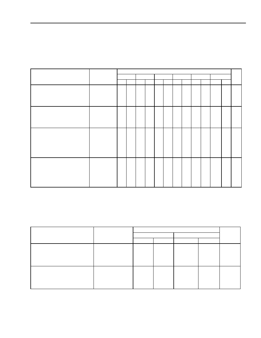
Table 39A. OR2CxxA and OR2TxxA Synchronous Memory Write Characteristics (SSPM and SDPM Modes)
OR2CxxA Commercial: VDD = 5.0 V ± 5%, 0 °C
≤ TA ≤ 70 °C; OR2CxxA Industrial: VDD = 5.0 V ± 10%, –40 °C ≤ TA ≤ +85 °C.
OR2TxxA Commercial: VDD = 3.0 V to 3.6 V, 0 °C
≤ TA ≤ 70 °C; OR2TxxA Industrial: VDD = 3.0 V to 3.6 V, –40 °C ≤ TA ≤
+85 °C.
Parameter
Symbol
Speed
Unit
-2
-3
-4
-5
-6
-7
Min
Max
Min
Max
Min
Max
Min
Max
Min
Max
Min
Max
Write Operation for Fast-RAM Mode1:
Maximum Frequency
Clock Low Time
Clock High Time
Clock to Data Valid (CK to F[3:0])2
FFSCK
TFSCL
TFSCH
FMEMS_DEL
38.2
13.1
—
9.0
52.6
9.5
—
7.4
83.3
6.0
—
6.2
90.9
5.5
—
5.0
92.6
5.4
—
5.3
96.2
5.2
—
5.2
MHz
ns
Write Operation for Normal RAM Mode:
Maximum Frequency
Clock Low Time
Clock High Time
Clock to Data Valid (CK to F[3:0])
FSCK
TSCL
TSCH
MEMS_DEL
24.3
20.6
—
10.9
33.3
15.0
—
8.6
52.6
9.5
—
7.5
58.0
8.5
—
6.0
58.8
8.5
—
6.4
59.8
8.4
—
5.9
MHz
ns
Write Operation Setup Time:
Address to Clock (A[3:0]/B[3:0] to CK)
Data to Clock (WD[3:0] to CK)
Write Enable (WREN) to Clock
(A4 to CK)
Write-port Enable (WPE) to Clock
(C0 to CK)
MEMS_ASET
MEMS_DSET
MEMS_WRSET
MEMS_PWRSET
0.0
—
0.0
—
0.0
—
0.0
—
0.0
—
0.0
—
ns
Write Operation Hold Time:
Address to Clock (A[3:0]/B[3:0] to CK)
Data to Clock (WD[3:0] to CK)
Write Enable (WREN) to Clock
(A4 to CK)
Write-port Enable (WPE) to Clock
(C0 to CK)
MEMS_AHLD
MEMS_DHLD
MEMS_WRHLD
MEMS_PWRHLD
3.8
3.3
—
3.0
2.3
—
2.2
1.5
—
2.0
1.4
—
1.9
—
1.8
1.2
—
ns
Table 39.B OR2TxxB Synchronous Memory Write Characteristics (SSPM and SDPM Modes)
OR2TxxB Commercial: VDD = 3.0 V to 3.6 V, 0 °C
≤ TA ≤ 70 °C; OR2TxxB Industrial: VDD = 3.0 V to 3.6 V, –40 °C ≤ TA ≤ +85°C.
Parameter
Symbol
Speed
Unit
-7
-8
Min
Max
Min
Max
Write Operation for Fast-RAM Mode1:
Maximum Frequency
Clock Low Time
Clock High Time
Clock to Data Valid (CK to F[3:0])2
FFSCK
TFSCL
TFSCH
FMEMS_DEL
97.7
5.1
—
5.1
112.4
4.5
—
4.5
MHz
ns
Write Operation for Normal RAM Mode:
Maximum Frequency
Clock Low Time
Clock High Time
Clock to Data Valid (CK to F[3:0])
FSCK
TSCL
TSCH
MEMS_DEL
60.8
8.2
—
5.1
69.9
7.2
—
4.5
MHz
ns
相关PDF资料 |
PDF描述 |
|---|---|
| OR2T26A-6T240I | Field-Programmable Gate Arrays |
| OR2T26A-6T304 | Field-Programmable Gate Arrays |
| OR2T26A-6T304I | Field-Programmable Gate Arrays |
| OR2T26A-6T352 | Field-Programmable Gate Arrays |
| OR2T26A-6T352I | Ceramic Chip Capacitors / MIL-PRF-55681; Capacitance [nom]: 9100pF; Working Voltage (Vdc)[max]: 50V; Capacitance Tolerance: +/-1%; Dielectric: Multilayer Ceramic; Temperature Coefficient: C0G (NP0); Lead Style: Surface Mount Chip; Lead Dimensions: 1812; Termination: Solder Coated SnPb; Body Dimensions: 0.180" x 0.125" x 0.080"; Container: Bag; Features: MIL-PRF-55681: S Failure Rate |
相关代理商/技术参数 |
参数描述 |
|---|---|
| OR2T26A7BA352-DB | 功能描述:FPGA - 现场可编程门阵列 2304 LUT 326 I/O RoHS:否 制造商:Altera Corporation 系列:Cyclone V E 栅极数量: 逻辑块数量:943 内嵌式块RAM - EBR:1956 kbit 输入/输出端数量:128 最大工作频率:800 MHz 工作电源电压:1.1 V 最大工作温度:+ 70 C 安装风格:SMD/SMT 封装 / 箱体:FBGA-256 |
| OR2T26A7BC432-DB | 功能描述:FPGA - 现场可编程门阵列 2304 LUT 326 I/O RoHS:否 制造商:Altera Corporation 系列:Cyclone V E 栅极数量: 逻辑块数量:943 内嵌式块RAM - EBR:1956 kbit 输入/输出端数量:128 最大工作频率:800 MHz 工作电源电压:1.1 V 最大工作温度:+ 70 C 安装风格:SMD/SMT 封装 / 箱体:FBGA-256 |
| OR2T26A7PS208-DB | 功能描述:FPGA - 现场可编程门阵列 2304 LUT 326 I/O RoHS:否 制造商:Altera Corporation 系列:Cyclone V E 栅极数量: 逻辑块数量:943 内嵌式块RAM - EBR:1956 kbit 输入/输出端数量:128 最大工作频率:800 MHz 工作电源电压:1.1 V 最大工作温度:+ 70 C 安装风格:SMD/SMT 封装 / 箱体:FBGA-256 |
| OR2T26A7PS240-DB | 功能描述:FPGA - 现场可编程门阵列 2304 LUT 326 I/O RoHS:否 制造商:Altera Corporation 系列:Cyclone V E 栅极数量: 逻辑块数量:943 内嵌式块RAM - EBR:1956 kbit 输入/输出端数量:128 最大工作频率:800 MHz 工作电源电压:1.1 V 最大工作温度:+ 70 C 安装风格:SMD/SMT 封装 / 箱体:FBGA-256 |
| OR2T26A7S208-DB | 功能描述:FPGA - 现场可编程门阵列 Use LatticeEC RoHS:否 制造商:Altera Corporation 系列:Cyclone V E 栅极数量: 逻辑块数量:943 内嵌式块RAM - EBR:1956 kbit 输入/输出端数量:128 最大工作频率:800 MHz 工作电源电压:1.1 V 最大工作温度:+ 70 C 安装风格:SMD/SMT 封装 / 箱体:FBGA-256 |
发布紧急采购,3分钟左右您将得到回复。