- 您现在的位置:买卖IC网 > PDF目录299576 > OR3T55-4PS208 FPGA, 324 CLBS, 40000 GATES, 80 MHz, PQFP208 PDF资料下载
参数资料
| 型号: | OR3T55-4PS208 |
| 元件分类: | FPGA |
| 英文描述: | FPGA, 324 CLBS, 40000 GATES, 80 MHz, PQFP208 |
| 封装: | SQFP-208 |
| 文件页数: | 171/210页 |
| 文件大小: | 2138K |
| 代理商: | OR3T55-4PS208 |
第1页第2页第3页第4页第5页第6页第7页第8页第9页第10页第11页第12页第13页第14页第15页第16页第17页第18页第19页第20页第21页第22页第23页第24页第25页第26页第27页第28页第29页第30页第31页第32页第33页第34页第35页第36页第37页第38页第39页第40页第41页第42页第43页第44页第45页第46页第47页第48页第49页第50页第51页第52页第53页第54页第55页第56页第57页第58页第59页第60页第61页第62页第63页第64页第65页第66页第67页第68页第69页第70页第71页第72页第73页第74页第75页第76页第77页第78页第79页第80页第81页第82页第83页第84页第85页第86页第87页第88页第89页第90页第91页第92页第93页第94页第95页第96页第97页第98页第99页第100页第101页第102页第103页第104页第105页第106页第107页第108页第109页第110页第111页第112页第113页第114页第115页第116页第117页第118页第119页第120页第121页第122页第123页第124页第125页第126页第127页第128页第129页第130页第131页第132页第133页第134页第135页第136页第137页第138页第139页第140页第141页第142页第143页第144页第145页第146页第147页第148页第149页第150页第151页第152页第153页第154页第155页第156页第157页第158页第159页第160页第161页第162页第163页第164页第165页第166页第167页第168页第169页第170页当前第171页第172页第173页第174页第175页第176页第177页第178页第179页第180页第181页第182页第183页第184页第185页第186页第187页第188页第189页第190页第191页第192页第193页第194页第195页第196页第197页第198页第199页第200页第201页第202页第203页第204页第205页第206页第207页第208页第209页第210页
Lucent Technologies Inc.
63
Preliminary Data Sheet, Rev. 1
September 1998
ORCA Series 3 FPGAs
Microprocessor Interface (MPI) (continued)
i960 System
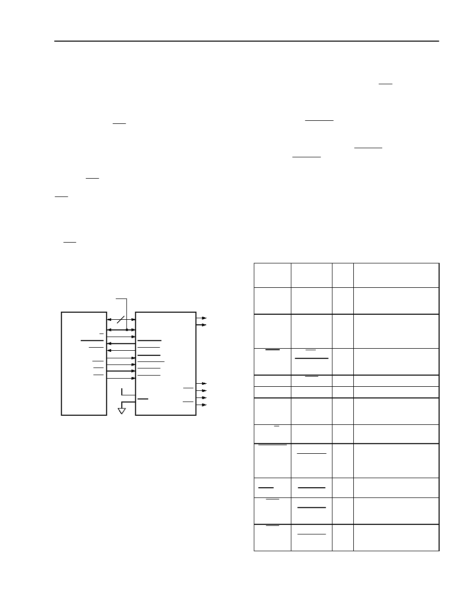
Figure 44 shows a schematic for connecting the
ORCA
MPI
to supported
i960 processors. In the figure, the
FPGA is shown as the only peripheral, with the FPGA
chip select lines, CS0 and CS1, tied low and high,
respectively. The
i960 address and data are multi-
plexed onto the same bus. This precludes memory
mapping of the FPGA in the
i960 memory space of a
multiperipheral system without some form of address
latching to capture and hold the address signals to
drive the CS0 and/or CS1 signals. Multiple address sig-
nals could also be decoded and latched to drive the
CS0
and/or CS1 signals. If the MPI is not used for
FPGA configuration, decoding/latching logic can be
implemented internal or external to the FPGA. If logic
internal to the FPGA is used, the chip selects must be
routed out an output pin and then connected externally
to CS0 and/or CS1. If the MPI is to be used for configu-
ration, any decode/latch logic used must be imple-
mented external to the FPGA since the FPGA logic has
not been configured yet.
5-5762(F)
Note: FPGA shown as only system peripheral with fixed-chip select
signals. For multiperipheral systems, address decoding and/or
latching can be used to implement chip selects.
Figure 44.
i960/MPI
The basic flow of a transaction on the
i960/MPI inter-
face is given below. Pin descriptions are shown in
Table 17, and timing is shown in the
ORCA Timing
Characteristics section of this data sheet. For both read
and write transactions, the address latch enable (ALE)
is set up by the
i960 at the FPGA to the falling edge of
the clock. The address, byte enables, chip selects, and
read/write (read low, write high) signals are normally
set up at the FPGA pins by the
i960 at the next rising
edge of the clock. At this same rising clock edge, the
i960 asserts its address/data strobe (ADS) low. Data is
available to the MPI during a write at the rising clock
edge of the following clock cycle. The transfer is
acknowledged to the
i960 by the low assertion of the
ready/recover (RDYRCV) signal. The same process
applies to a read from the MPI except that the read data
is expected at the FPGA data pins by the
i960 at the
rising edge of the clock when RDYRCV is low. The MPI
only drives RDYRCV low for one clock cycle.
Interrupts can be sent to the
i960 asynchronously to the
read/write process. Interrupt requests are sourced by
the user-logic in the FPGA. The MPI will assert the
request to the
i960 as a direct interrupt signal and/or a
pollable bit in the MPI status register (discussed in the
MPI
Setup and Control section). The MPI will continue
to assert the interrupt request until the user-logic deas-
serts its interrupt request signal.
DOUT
CCLK
D[7:0]
MPI_CLK
MPI_RW
MPI_ACK
MPI_IRQ
MPI_ALE
MPI_BE1
HDC
LDC
TO DAISY-
CHAINED
DEVICES
ORCA
8
FPGA
SERIES 3
DONE
INIT
AD[7:0]
CLKIN
W/R
RDYRCV
XINTx
ALE
BE1
i960
CS1
CS0
i960 SYSTEM CLOCK
VDD
MPI_BE0
BE0
MPI_STRB
ADS
Table 17.
i960/MPI Configuration
i960
Signal
ORCA Pin
Name
MPI
I/O
Function
AD[7:0]
D[7:0]
I/O
Multiplexed 5-bit address/
8-bit data bus. The
address appears on D[4:0].
ALE
RDY/RCLK/
MPI_ALE
I
Address latch enable used
to capture address from
AD[4:0] on falling edge of
clock.
ADS
RD
/
MPI_STRB
I
Address/data strobe to
indicate start of transac-
tion.
—
CS0
I
Active-low
MPI select.
—
CS1
I
Active-high
MPI select.
System
Clock
A7/
MPI_CLK
I
i960 system clock. This
clock is sourced by the
system and not the
i960.
W/R
A8/MPI_RW
I
Write (high)/read (low)
signal.
RDYRCV
A9/
MPI_ACK
O
Active-low ready/recover
signal indicating acknowl-
edgment of the transac-
tion.
Any of
XINT
[7:0]
A11/
MPI_IRQ
O
Active-low interrupt
request signal.
BE0
A0/
MPI_BE0
I
Byte-enable 0 used as
address bit 0 in
i960 8-bit
mode.
BE1
A1/
MPI_BE1
I
Byte-enable 1 used as
address bit 1 in
i960 8-bit
mode.
相关PDF资料 |
PDF描述 |
|---|---|
| OR3T80-4PS208I | FPGA, 484 CLBS, 58000 GATES, 80 MHz, PQFP208 |
| OR3T80-4PS208 | FPGA, 484 CLBS, 58000 GATES, 80 MHz, PQFP208 |
| OR3T125-4PS240I | FPGA, 784 CLBS, 92000 GATES, 80 MHz, PQFP240 |
| OR3T125-4PS240 | FPGA, 784 CLBS, 92000 GATES, 80 MHz, PQFP240 |
| OR3T55-4PS240I | FPGA, 324 CLBS, 40000 GATES, 80 MHz, PQFP240 |
相关代理商/技术参数 |
参数描述 |
|---|---|
| OR3T55-4PS208I | 制造商:未知厂家 制造商全称:未知厂家 功能描述:Field Programmable Gate Array (FPGA) |
| OR3T55-4PS240I | 制造商:未知厂家 制造商全称:未知厂家 功能描述:Field Programmable Gate Array (FPGA) |
| OR3T55-5BA256 | 制造商:AGERE 制造商全称:AGERE 功能描述:3C and 3T Field-Programmable Gate Arrays |
| OR3T55-5BA256I | 制造商:AGERE 制造商全称:AGERE 功能描述:3C and 3T Field-Programmable Gate Arrays |
| OR3T55-5BA352 | 制造商:AGERE 制造商全称:AGERE 功能描述:3C and 3T Field-Programmable Gate Arrays |
发布紧急采购,3分钟左右您将得到回复。