- 您现在的位置:买卖IC网 > PDF目录11731 > ORSO42G5-1BM484I (Lattice Semiconductor Corporation)IC FPSC TRANSCEIVER 4CH 484-BGA PDF资料下载
参数资料
| 型号: | ORSO42G5-1BM484I |
| 厂商: | Lattice Semiconductor Corporation |
| 文件页数: | 69/153页 |
| 文件大小: | 0K |
| 描述: | IC FPSC TRANSCEIVER 4CH 484-BGA |
| 产品变化通告: | Product Discontinuation 01/Aug/2011 |
| 标准包装: | 60 |
| 系列: | * |
第1页第2页第3页第4页第5页第6页第7页第8页第9页第10页第11页第12页第13页第14页第15页第16页第17页第18页第19页第20页第21页第22页第23页第24页第25页第26页第27页第28页第29页第30页第31页第32页第33页第34页第35页第36页第37页第38页第39页第40页第41页第42页第43页第44页第45页第46页第47页第48页第49页第50页第51页第52页第53页第54页第55页第56页第57页第58页第59页第60页第61页第62页第63页第64页第65页第66页第67页第68页当前第69页第70页第71页第72页第73页第74页第75页第76页第77页第78页第79页第80页第81页第82页第83页第84页第85页第86页第87页第88页第89页第90页第91页第92页第93页第94页第95页第96页第97页第98页第99页第100页第101页第102页第103页第104页第105页第106页第107页第108页第109页第110页第111页第112页第113页第114页第115页第116页第117页第118页第119页第120页第121页第122页第123页第124页第125页第126页第127页第128页第129页第130页第131页第132页第133页第134页第135页第136页第137页第138页第139页第140页第141页第142页第143页第144页第145页第146页第147页第148页第149页第150页第151页第152页第153页
Lattice Semiconductor
ORCA ORSO42G5 and ORSO82G5 Data Sheet
22
Since this effect is predictable for a given type of PCB material, it is possible to compensate for this effect in two
ways - transmitter preemphasis and receiver equalization. Each of these techniques boosts the high frequency
components of the signal but transmit preemphasis is preferred due to the ease of implementation and the better
power utilization. It also gives a better signal-to-noise ratio because receiver equalization amplies both the signal
and the noise at the receiver.
Applying too much preemphasis when it is not required, for example when driving a short backplane path, will also
degrade the data eye opening at the receiver. In the ORSO42G5 and ORSO82G5, the degree of transmit preem-
phasis can be programmed per channel with two control register bits as shown in Table 4. The high-pass transfer
function of the preemphasis circuit is given by the following equation, where the value of a is shown in Table 4.
H(z) = (1 – az
–1)
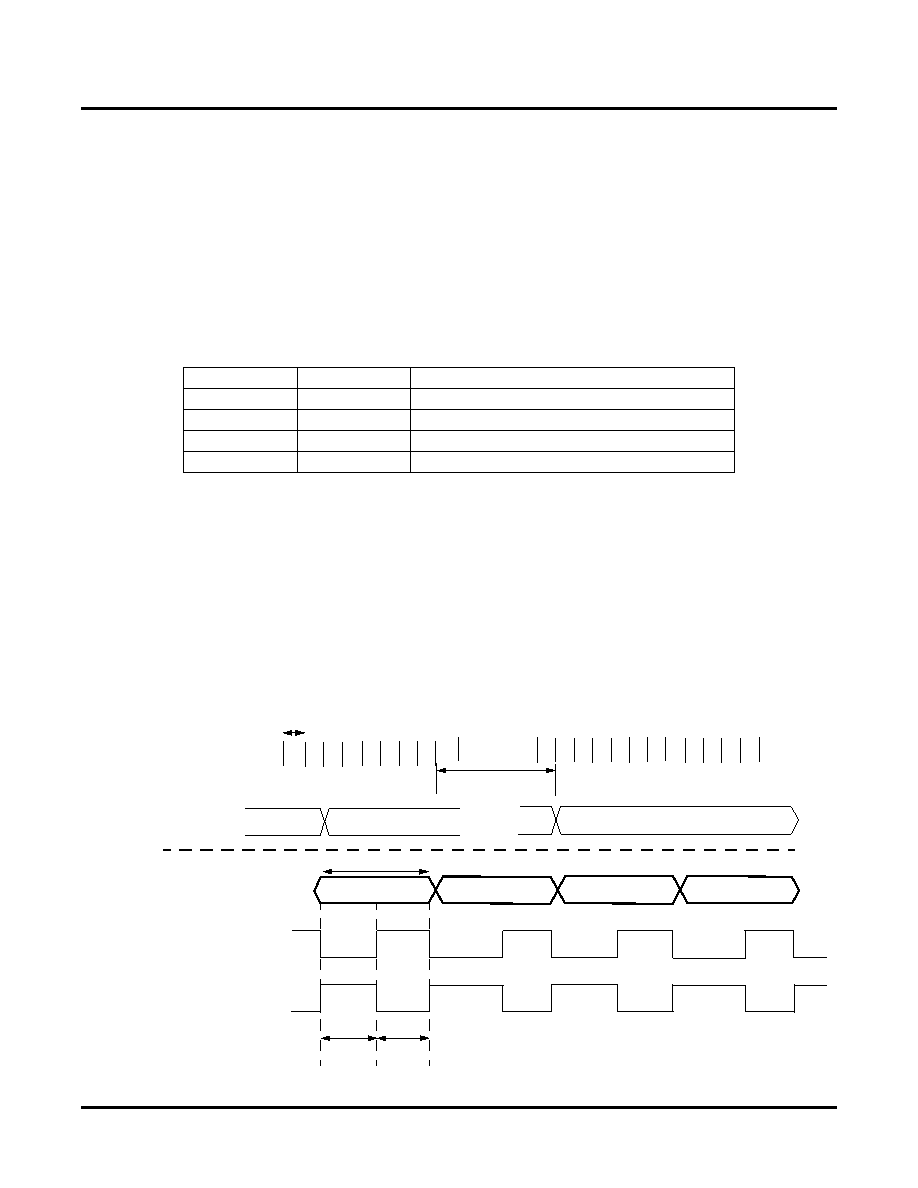
Table 4. Preemphasis Settings
SERDES Receive Path
The receiver section receives high-speed serial data at its differential CML input port. These data are fed to the
clock recovery section which generates a recovered clock and retimes the data. Each SERDES receive channel
has its own PLL and this means that the receive clocks are asynchronous between channels. This also enables
each receive channel to either operate in half-rate or full-rate mode.The retimed data are deserialized and pre-
sented as a 8-bit parallel data on the output port. Two-phase receive byte clocks (RBC0 and RBC1) are available
synchronous with the parallel words. RBC0 has its rising edge aligned to the center of the receive byte. RBC1 has
its falling edge aligned to the center of the receive byte. The 8-bit data (LDOUT) as shown in Figure 8, changes on
a single clock edge (rising edge of RBC0 or falling edge of RBC1).
Figure 8. SERDES Receive Path Timing
PE1
PE0
Amount of Preemphasis (a)
0
0% (No Preemphasis, Default)
0
1
12.5%
1
0
12.5%
1
25%
.....
LDOUT[7:0]
RBC0x
RBC1x
q
7
r
1
r
0
s
7
p
3
p
2
p
1
p
0
.....
p
7
p
6
p
5
p
4
r
7
r
6
r
5
r
4
r
3
r
2
s
6
s
5
s
4
s
3
p
HDINx
LDOUT[7:0]
1-bit
8-bit
.....
LATENCY
p
q
r
s
SETUP
HOLD
相关PDF资料 |
PDF描述 |
|---|---|
| PIC18F4682-I/ML | IC PIC MCU FLASH 40KX16 44QFN |
| ORT8850L-2BMN680I | IC TRANCEIVERS FPSC 680FPGAM |
| ORT8850L-1BMN680C | IC TRANCEIVERS FPSC 680FPGAM |
| VE-B0B-IX-F1 | CONVERTER MOD DC/DC 95V 75W |
| SY100E446JC TR | IC CONV 4-BIT SER/PAR 28-PLCC |
相关代理商/技术参数 |
参数描述 |
|---|---|
| ORSO42G5-1BMN484C | 功能描述:FPGA - 现场可编程门阵列 10368 LUT 204 I/O RoHS:否 制造商:Altera Corporation 系列:Cyclone V E 栅极数量: 逻辑块数量:943 内嵌式块RAM - EBR:1956 kbit 输入/输出端数量:128 最大工作频率:800 MHz 工作电源电压:1.1 V 最大工作温度:+ 70 C 安装风格:SMD/SMT 封装 / 箱体:FBGA-256 |
| ORSO42G5-1BMN484I | 功能描述:FPGA - 现场可编程门阵列 10368 LUT 204 I/O RoHS:否 制造商:Altera Corporation 系列:Cyclone V E 栅极数量: 逻辑块数量:943 内嵌式块RAM - EBR:1956 kbit 输入/输出端数量:128 最大工作频率:800 MHz 工作电源电压:1.1 V 最大工作温度:+ 70 C 安装风格:SMD/SMT 封装 / 箱体:FBGA-256 |
| ORSO42G5-2BM484C | 功能描述:FPGA - 现场可编程门阵列 10368 LUT 204 I/O RoHS:否 制造商:Altera Corporation 系列:Cyclone V E 栅极数量: 逻辑块数量:943 内嵌式块RAM - EBR:1956 kbit 输入/输出端数量:128 最大工作频率:800 MHz 工作电源电压:1.1 V 最大工作温度:+ 70 C 安装风格:SMD/SMT 封装 / 箱体:FBGA-256 |
| ORSO42G5-2BM484I | 功能描述:FPGA - 现场可编程门阵列 10368 LUT 204 I/O RoHS:否 制造商:Altera Corporation 系列:Cyclone V E 栅极数量: 逻辑块数量:943 内嵌式块RAM - EBR:1956 kbit 输入/输出端数量:128 最大工作频率:800 MHz 工作电源电压:1.1 V 最大工作温度:+ 70 C 安装风格:SMD/SMT 封装 / 箱体:FBGA-256 |
| ORSO42G5-2BMN484C | 功能描述:FPGA - 现场可编程门阵列 10368 LUT 204 I/O RoHS:否 制造商:Altera Corporation 系列:Cyclone V E 栅极数量: 逻辑块数量:943 内嵌式块RAM - EBR:1956 kbit 输入/输出端数量:128 最大工作频率:800 MHz 工作电源电压:1.1 V 最大工作温度:+ 70 C 安装风格:SMD/SMT 封装 / 箱体:FBGA-256 |
发布紧急采购,3分钟左右您将得到回复。