参数资料
| 型号: | P6SMB68AT3G |
| 厂商: | ON Semiconductor |
| 文件页数: | 4/6页 |
| 文件大小: | 0K |
| 描述: | TVS ZENER UNIDIR 600W 68V SMB |
| 产品目录绘图: | 1SMB, P6SMB Series |
| 标准包装: | 10 |
| 电压 - 反向隔离(标准值): | 58.1V |
| 电压 - 击穿: | 64.6V |
| 功率(瓦特): | 600W |
| 电极标记: | 单向 |
| 安装类型: | 表面贴装 |
| 封装/外壳: | DO-214AA,SMB |
| 供应商设备封装: | SMB |
| 包装: | 标准包装 |
| 产品目录页面: | 2380 (CN2011-ZH PDF) |
| 其它名称: | P6SMB68AT3GOSDKR |
�� �
�
�P6SMB11CAT3G� Series,� SZP6SMB11CAT3G� Series�
�APPLICATION� NOTES�
�Response� Time�
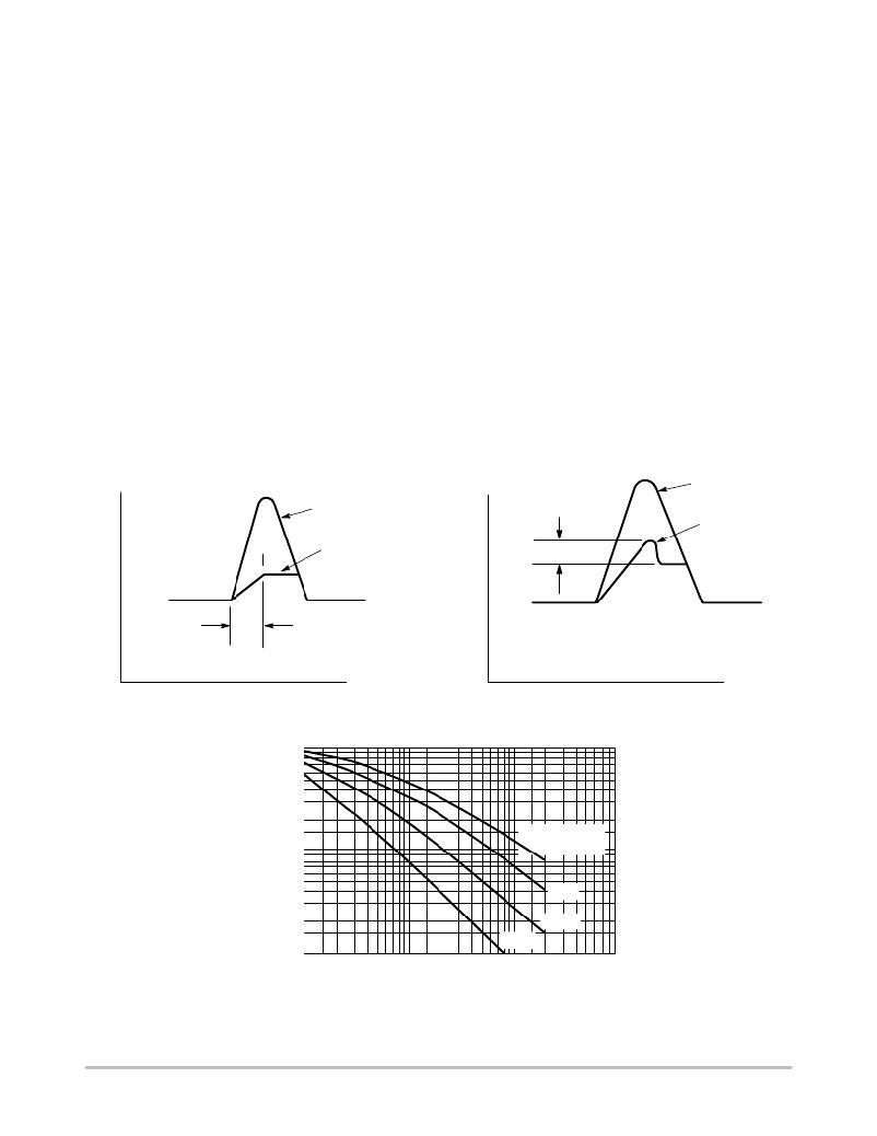
�In� most� applications,� the� transient� suppressor� device� is�
�placed� in� parallel� with� the� equipment� or� component� to� be�
�protected.� In� this� situation,� there� is� a� time� delay� associated� with�
�the� capacitance� of� the� device� and� an� overshoot� condition�
�associated� with� the� inductance� of� the� device� and� the� inductance�
�of� the� connection� method.� The� capacitive� effect� is� of� minor�
�importance� in� the� parallel� protection� scheme� because� it� only�
�produces� a� time� delay� in� the� transition� from� the� operating�
�voltage� to� the� clamp� voltage� as� shown� in� Figure� 4.�
�The� inductive� effects� in� the� device� are� due� to� actual� turn-on�
�time� (time� required� for� the� device� to� go� from� zero� current� to� full�
�current)� and� lead� inductance.� This� inductive� effect� produces� an�
�overshoot� in� the� voltage� across� the� equipment� or� component�
�being� protected� as� shown� in� Figure� 5.� Minimizing� this�
�overshoot� is� very� important� in� the� application,� since� the� main�
�purpose� for� adding� a� transient� suppressor� is� to� clamp� voltage�
�spikes.� The� SMB� series� have� a� very� good� response� time,�
�typically� <� 1� ns� and� negligible� inductance.� However,� external�
�inductive� effects� could� produce� unacceptable� overshoot.�
�Proper� circuit� layout,� minimum� lead� lengths� and� placing� the�
�suppressor� device� as� close� as� possible� to� the� equipment� or�
�components� to� be� protected� will� minimize� this� overshoot.�
�Some� input� impedance� represented� by� Z� in� is� essential� to�
�prevent� overstress� of� the� protection� device.� This� impedance�
�should� be� as� high� as� possible,� without� restricting� the� circuit�
�operation.�
�Duty� Cycle� Derating�
�The� data� of� Figure� 1� applies� for� non-repetitive� conditions�
�and� at� a� lead� temperature� of� 25� ?� C.� If� the� duty� cycle� increases,�
�the� peak� power� must� be� reduced� as� indicated� by� the� curves� of�
�Figure� 6.� Average� power� must� be� derated� as� the� lead� or� ambient�
�temperature� rises� above� 25� ?� C.� The� average� power� derating�
�curve� normally� given� on� data� sheets� may� be� normalized� and�
�used� for� this� purpose.�
�At� first� glance� the� derating� curves� of� Figure� 6� appear� to� be�
�in� error� as� the� 10� ms� pulse� has� a� higher� derating� factor� than�
�the� 10� m� s� pulse.� However,� when� the� derating� factor� for� a�
�given� pulse� of� Figure� 6� is� multiplied� by� the� peak� power� value�
�of� Figure� 1� for� the� same� pulse,� the� results� follow� the�
�expected� trend.�
�V�
�V� in� (TRANSIENT)�
�V�
�OVERSHOOT� DUE� TO�
�INDUCTIVE� EFFECTS�
�V� in� (TRANSIENT)�
�V� L�
�V� L�
�V� in�
�t� d�
�t� D� =� TIME� DELAY� DUE� TO� CAPACITIVE� EFFECT�
�Figure� 5.�
�1�
�0.7�
�0.5�
�0.3�
�0.2�
�0.1�
�0.07�
�0.05�
�0.03�
�0.02�
�t�
�Figure� 6.�
�PULSE� WIDTH�
�10� ms�
�1� ms�
�100� m� s�
�t�
�0.01�
�0.1� 0.2�
�0.5�
�1�
�10� m� s�
�2� 5� 10�
�20�
�50� 100�
�D,� DUTY� CYCLE� (%)�
�Figure� 7.� Typical� Derating� Factor� for� Duty� Cycle�
�http://onsemi.com�
�4�
�相关PDF资料 |
PDF描述 |
|---|---|
| 76382-406LF | CONN HEADER 6POS .100" R/A TIN |
| 963260-2000-AR-PR | CONN SOCKET DUAL 60POS GOLD SMD |
| SFML-115-02-L-D | CONN RECEPT 30POS .50" SMT |
| ESQ-112-44-G-D | CONN RCPT 24POS .100" DUAL GOLD |
| 950462-6102-AR | CONN SOCKET 62POS 2MM VERT PCB |
相关代理商/技术参数 |
参数描述 |
|---|---|
| P6SMB68AT3G | 制造商:ON Semiconductor 功能描述:ZENER DIODE |
| P6SMB68C | 功能描述:TVS 二极管 - 瞬态电压抑制器 TVS SURF MT DO214AA RoHS:否 制造商:Vishay Semiconductors 极性:Bidirectional 工作电压: 击穿电压:58.9 V 钳位电压:77.4 V 峰值浪涌电流:38.8 A 系列: 封装 / 箱体:DO-214AB 最小工作温度:- 55 C 最大工作温度:+ 150 C |
| P6SMB68CA | 功能描述:TVS 二极管 - 瞬态电压抑制器 TVS SURF MT DO214AA RoHS:否 制造商:Vishay Semiconductors 极性:Bidirectional 工作电压: 击穿电压:58.9 V 钳位电压:77.4 V 峰值浪涌电流:38.8 A 系列: 封装 / 箱体:DO-214AB 最小工作温度:- 55 C 最大工作温度:+ 150 C |
| P6SMB68CA R4 | 制造商:SKMI/Taiwan 功能描述:Diode TVS Single Bi-Dir 58.1V 600W 2-Pin SMB T/R |
| P6SMB68CA/2 | 功能描述:TVS 二极管 - 瞬态电压抑制器 600W 68V Bidirect RoHS:否 制造商:Vishay Semiconductors 极性:Bidirectional 工作电压: 击穿电压:58.9 V 钳位电压:77.4 V 峰值浪涌电流:38.8 A 系列: 封装 / 箱体:DO-214AB 最小工作温度:- 55 C 最大工作温度:+ 150 C |
发布紧急采购,3分钟左右您将得到回复。