参数资料
| 型号: | P87C54X2BA,512 |
| 厂商: | NXP Semiconductors |
| 文件页数: | 2/62页 |
| 文件大小: | 0K |
| 描述: | IC 80C51 MCU 256 RAM 44PLCC |
| 产品培训模块: | Migrating from 8/16-Bit MCUs to 32-Bit ARMs |
| 标准包装: | 26 |
| 系列: | 87C |
| 核心处理器: | 8051 |
| 芯体尺寸: | 8-位 |
| 速度: | 33MHz |
| 连通性: | EBI/EMI,UART/USART |
| 外围设备: | POR |
| 输入/输出数: | 32 |
| 程序存储器容量: | 16KB(16K x 8) |
| 程序存储器类型: | OTP |
| RAM 容量: | 256 x 8 |
| 电压 - 电源 (Vcc/Vdd): | 2.7 V ~ 5.5 V |
| 振荡器型: | 内部 |
| 工作温度: | 0°C ~ 70°C |
| 封装/外壳: | 44-LCC(J 形引线) |
| 包装: | 管件 |
| 其它名称: | 568-7913-5 568-7913-5-ND 568-8362-5 935270161512 P87C54X2BA P87C54X2BA,512-ND P87C54X2BA-ND |
第1页当前第2页第3页第4页第5页第6页第7页第8页第9页第10页第11页第12页第13页第14页第15页第16页第17页第18页第19页第20页第21页第22页第23页第24页第25页第26页第27页第28页第29页第30页第31页第32页第33页第34页第35页第36页第37页第38页第39页第40页第41页第42页第43页第44页第45页第46页第47页第48页第49页第50页第51页第52页第53页第54页第55页第56页第57页第58页第59页第60页第61页第62页
Philips Semiconductors
Product data
P80C3xX2; P80C5xX2;
P87C5xX2
80C51 8-bit microcontroller family
4K/8K/16K/32K ROM/OTP, low voltage (2.7 to 5.5 V),
low power, high speed (30/33 MHz)
2003 Jan 24
10
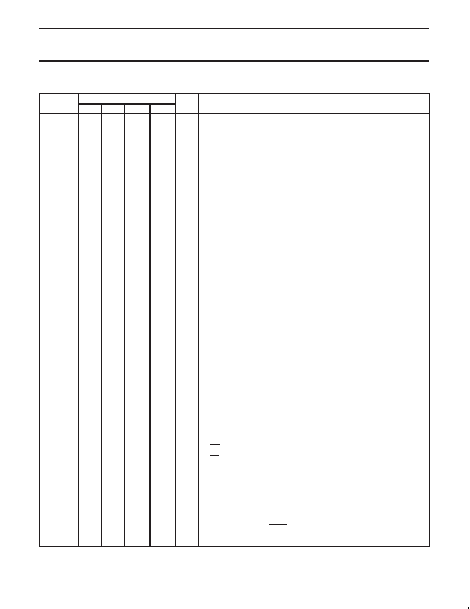
PIN DESCRIPTIONS
PIN NUMBER
MNEMONIC
DIP
PLCC
LQFP
TSSOP
TYPE
NAME AND FUNCTION
VSS
20
22
16
9
I
Ground: 0 V reference.
VCC
40
44
38
29
I
Power Supply: This is the power supply voltage for normal, idle, and power-down
operation.
P0.0-0.7
39–32
43–36
37–30
28–21
I/O
Port 0: Port 0 is an open-drain, bidirectional I/O port. Port 0 pins that have 1s
written to them float and can be used as high-impedance inputs. Port 0 is also the
multiplexed low-order address and data bus during accesses to external program
and data memory. In this application, it uses strong internal pull-ups when emitting
1s. Port 0 also outputs the code bytes during program verification and received
code bytes during EPROM programming. External pull-ups are required during
program verification.
P1.0–P1.7
1–8
2–9
40–44,
1–3
30–37
I/O
Port 1: Port 1 is an 8-bit bidirectional I/O port with internal pull-ups. Port 1 pins that
have 1s written to them are pulled high by the internal pull-ups and can be used as
inputs. As inputs, port 1 pins that are externally pulled low will source current
because of the internal pull-ups. (See DC Electrical Characteristics: IIL). Port 1 also
receives the low-order address byte during program memory verification. Alternate
functions for Port 1 include:
1
2
40
30
I/O
T2 (P1.0): Timer/Counter 2 external count input/clockout (see Programmable
Clock-Out)
2
3
41
31
I
T2EX (P1.1): Timer/Counter 2 Reload/Capture/Direction control
P2.0–P2.7
21–28
24–31
18–25
10–17
I/O
Port 2: Port 2 is an 8-bit bidirectional I/O port with internal pull-ups. Port 2 pins that
have 1s written to them are pulled high by the internal pull-ups and can be used as
inputs. As inputs, port 2 pins that are externally being pulled low will source current
because of the internal pull-ups. (See DC Electrical Characteristics: IIL). Port 2
emits the high-order address byte during fetches from external program memory
and during accesses to external data memory that use 16-bit addresses (MOVX
@DPTR). In this application, it uses strong internal pull-ups when emitting 1s.
During accesses to external data memory that use 8-bit addresses (MOV @Ri), port
2 emits the contents of the P2 special function register. Some Port 2 pins receive
the high order address bits during EPROM programming and verification.
P3.0–P3.7
10–17
11,
13–19
5,
7–13
1–6
I/O
Port 3: Port 3 is an 8-bit bidirectional I/O port with internal pull-ups. Port 3 pins that
have 1s written to them are pulled high by the internal pull-ups and can be used as
inputs. As inputs, port 3 pins that are externally being pulled low will source current
because of the pull-ups. (See DC Electrical Characteristics: IIL). Port 3 also serves
the special features of the 80C51 family, as listed below:
10
11
5
1
I
RxD (P3.0): Serial input port
11
13
7
2
O
TxD (P3.1): Serial output port
12
14
8
I
INT0 (P3.2): External interrupt1
13
15
9
3
I
INT1 (P3.3): External interrupt
14
16
10
4
I
T0 (P3.4): Timer 0 external input
15
17
11
I
T1 (P3.5): Timer 1 external input1
16
18
12
5
O
WR (P3.6): External data memory write strobe
17
19
13
6
O
RD (P3.7): External data memory read strobe
RST
9
10
4
38
I
Reset: A high on this pin for two machine cycles while the oscillator is running,
resets the device. An internal diffused resistor to VSS permits a power-on reset
using only an external capacitor to VCC.
ALE/PROG
30
33
27
19
O
Address Latch Enable/Program Pulse: Output pulse for latching the low byte of
the address during an access to external memory. In normal operation, ALE is
emitted at a constant rate of 1/6 (12-clock Mode) or 1/3 (6-clock Mode) the
oscillator frequency, and can be used for external timing or clocking. Note that one
ALE pulse is skipped during each access to external data memory. This pin is also
the program pulse input (PROG) during EPROM programming. ALE can be
disabled by setting SFR auxiliary.0. With this bit set, ALE will be active only during
a MOVX instruction.
相关PDF资料 |
PDF描述 |
|---|---|
| P87LPC764BN,112 | IC 80C51 MCU 4K OTP 20-DIP |
| C8051F920-GQ | IC 8051 MCU 32K FLASH 32-LQFP |
| LPC1313FBD48/01,15 | MCU CORTEX M3 32KB FLASH 48-LQFP |
| P80C32SBPN,112 | IC 80C51 MCU 256X8 ROMLESS 40DIP |
| P89LPC985FA,529 | IC 80C51 MCU 8KB FLASH 28PLCC |
相关代理商/技术参数 |
参数描述 |
|---|---|
| P87C54X2BBD | 制造商:PHILIPS 制造商全称:NXP Semiconductors 功能描述:80C51 8-bit microcontroller family 4K/8K/16K/32K ROM/OTP 128B/256B RAM low voltage 2.7 to 5.5 V, low power, high speed 30/33 MHz |
| P87C54X2BBD,157 | 功能描述:8位微控制器 -MCU 80C51 16K/256 OTP RoHS:否 制造商:Silicon Labs 核心:8051 处理器系列:C8051F39x 数据总线宽度:8 bit 最大时钟频率:50 MHz 程序存储器大小:16 KB 数据 RAM 大小:1 KB 片上 ADC:Yes 工作电源电压:1.8 V to 3.6 V 工作温度范围:- 40 C to + 105 C 封装 / 箱体:QFN-20 安装风格:SMD/SMT |
| P87C54X2BDH | 制造商:PHILIPS 制造商全称:NXP Semiconductors 功能描述:80C51 8-bit microcontroller family 4K/8K/16K/32K ROM/OTP 128B/256B RAM low voltage 2.7 to 5.5 V, low power, high speed 30/33 MHz |
| P87C54X2BN | 制造商:PHILIPS 制造商全称:NXP Semiconductors 功能描述:80C51 8-bit microcontroller family 4K/8K/16K/32K ROM/OTP 128B/256B RAM low voltage 2.7 to 5.5 V, low power, high speed 30/33 MHz |
| P87C54X2BN,112 | 功能描述:8位微控制器 -MCU 80C51 16K/256 OTP RoHS:否 制造商:Silicon Labs 核心:8051 处理器系列:C8051F39x 数据总线宽度:8 bit 最大时钟频率:50 MHz 程序存储器大小:16 KB 数据 RAM 大小:1 KB 片上 ADC:Yes 工作电源电压:1.8 V to 3.6 V 工作温度范围:- 40 C to + 105 C 封装 / 箱体:QFN-20 安装风格:SMD/SMT |
发布紧急采购,3分钟左右您将得到回复。