- 您现在的位置:买卖IC网 > PDF目录367738 > P87C552 (NXP Semiconductors N.V.) 80C51 8-bit microcontroller(80C51八位微控制器) PDF资料下载
参数资料
| 型号: | P87C552 |
| 厂商: | NXP Semiconductors N.V. |
| 英文描述: | 80C51 8-bit microcontroller(80C51八位微控制器) |
| 中文描述: | 80C51的8位微控制器(80C51的八位微控制器) |
| 文件页数: | 18/74页 |
| 文件大小: | 368K |
| 代理商: | P87C552 |
第1页第2页第3页第4页第5页第6页第7页第8页第9页第10页第11页第12页第13页第14页第15页第16页第17页当前第18页第19页第20页第21页第22页第23页第24页第25页第26页第27页第28页第29页第30页第31页第32页第33页第34页第35页第36页第37页第38页第39页第40页第41页第42页第43页第44页第45页第46页第47页第48页第49页第50页第51页第52页第53页第54页第55页第56页第57页第58页第59页第60页第61页第62页第63页第64页第65页第66页第67页第68页第69页第70页第71页第72页第73页第74页
Philips Semiconductors
Preliminary specification
P87C552
80C51 8-bit microcontroller
8K/256 OTP, 8 channel 10 bit A/D, I
2
C, PWM,
capture/compare, high I/O, low voltage (2.7V–5.5V), low power
1999 Mar 30
18
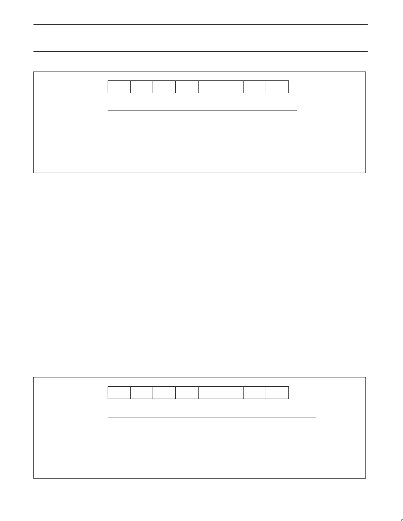
CTP0
BIT
SYMBOL
CAPTURE/INTERRUPT ON:
CTCON.7
CTCON.6
CTCON.5
CTCON.4
CTCON.3
CTCON.2
CTCON.1
CTCON.0
CTN3
CTP3
CTN2
CTP2
CTN1
CTP1
CTN0
CTP0
Capture Register 3 triggered by a falling edge on CT3I
Capture Register 3 triggered by a rising edge on CT3I
Capture Register 2 triggered by a falling edge on CT2I
Capture Register 2 triggered by a rising edge on CT2I
Capture Register 1 triggered by a falling edge on CT1I
Capture Register 1 triggered by a rising edge on CT1I
Capture Register 0 triggered by a falling edge on CT0I
Capture Register 0 triggered by a rising edge on CT0I
SU01085
CTN1
CTP1
CTN1
CTP2
CTN2
CTP3
CTN3
0
1
2
3
4
5
6
7
(LSB)
(MSB)
CTCON (EBH)
Reset Value = 00H
Figure 13. Capture Control Register (CTCON)
When a match with CM1 occurs, the controller resets bits 0-5 of port
4 if the corresponding bits of the reset/toggle enable register RTE
are at logic 1 (see Figure 14 for RTE register function). If RTE is “0”,
then P4.n is not affected by a match between CM1 or CM2 and
Timer 2. When a match with CM2 occurs, the controller “toggles”
bits 6 and 7 of port 4 if the corresponding bits of the RTE are at
logic 1. The port latches of bits 6 and 7 are not toggled.
Two additional flip-flops store the last operation, and it is these
flip-flops that are toggled.
Thus, if the current operation is “set,” the next operation will be
“reset” even if the port latch is reset by software before the “reset”
operation occurs. The first “toggle” after a chip RESET will set the
port latch. The contents of these two flip-flops can be read at STE.6
and STE.7 (corresponding to P4.6 and P4.7, respectively). Bits
STE.6 and STE.7 are read only (see Figure 15 for STE register
function). A logic 1 indicates that the next toggle will set the port
latch; a logic 0 indicates that the next toggle will reset the port latch.
CM0, CM1, and CM2 are reset by the RST signal.
The modified port latch information appears at the port pin during
S5P1 of the cycle following the cycle in which a match occurred. If
the port is modified by software, the outputs change during S1P1 of
the following cycle. Each port 4 bit can be set or reset by software at
any time. A hardware modification resulting from a comparator
match takes precedence over a software modification in the same
cycle. When the comparator results require a “set” and a “reset” at
the same time, the port latch will be reset.
Timer T2 Interrupt Flag Register TM2IR:
Eight of the nine Timer
T2 interrupt flags are located in special function register TM2IR (see
Figure 16). The ninth flag is TM2CON.4.
The CT0I and CT1I flags are set during S4 of the cycle in which the
contents of Timer T2 are captured. CT0I is scanned by the interrupt
logic during S2, and CT1I is scanned during S3. CT2I and CT3I are
set during S6 and are scanned during S4 and S5. The associated
interrupt requests are recognized during the following cycle. If these
flags are polled, a transition at CT0I or CT1I will be recognized one
cycle before a transition on CT2I or CT3I since registers are read
during S5. The CMI0, CMI1, and CMI2 flags are set during S6 of the
cycle following a match. CMI0 is scanned by the interrupt logic
during S2; CMI1 and CMI2 are scanned during S3 and S4. A match
will be recognized by the interrupt logic (or by polling the flags) two
cycles after the match takes place.
The 16-bit overflow flag (T2OV) and the byte overflow flag (T2BO)
are set during S6 of the cycle in which the overflow occurs. These
flags are recognized by the interrupt logic during the next cycle.
Special function register IP1 (Figure 16) is used to determine the
Timer T2 interrupt priority. Setting a bit high gives that function a
high priority, and setting a bit low gives the function a low priority.
The functions controlled by the various bits of the IP1 register are
shown in Figure 16.
RP40
BIT
SYMBOL
FUNCTION
RTE.7
RTE.6
RTE.5
RTE.4
RTE.3
RTE.2
RTE.1
RTE.0
TP47
TP46
RP45
RP44
RP43
RP42
RP41
RP40
If “1” then P4.7 toggles on a match between CM1 and Timer T2
If “1” then P4.6 toggles on a match between CM1 and Timer T2
If “1” then P4.5 is reset on a match between CM1 and Timer T2
If “1” then P4.4 is reset on a match between CM1 and Timer T2
If “1” then P4.3 is reset on a match between CM1 and Timer T2
If “1” then P4.2 is reset on a match between CM1 and Timer T2
If “1” then P4.1 is reset on a match between CM1 and Timer T2
If “1” then P4.0 is reset on a match between CM1 and Timer T2
SU01086
RO41
RP42
RP43
RP44
RP45
TP46
TP47
0
1
2
3
4
5
6
7
(LSB)
(MSB)
RTE (EFH)
Reset Value = 00H
Figure 14. Reset/Toggle Enable Register (RTE)
相关PDF资料 |
PDF描述 |
|---|---|
| P87C554SBBD | 80C51 8-bit microcontroller . 6 clock operation 16K/512 OTP/ROM/ROMless, 7 channel 10 bit A/D, I2C, PWM, capture/compare, high I/O, 64L LQFP |
| P83C554SBBD | 80C51 8-bit microcontroller . 6 clock operation 16K/512 OTP/ROM/ROMless, 7 channel 10 bit A/D, I2C, PWM, capture/compare, high I/O, 64L LQFP |
| P80C554SBBD | 80C51 8-bit microcontroller . 6 clock operation 16K/512 OTP/ROM/ROMless, 7 channel 10 bit A/D, I2C, PWM, capture/compare, high I/O, 64L LQFP |
| P87C554SFBD | 80C51 8-bit microcontroller . 6 clock operation 16K/512 OTP/ROM/ROMless, 7 channel 10 bit A/D, I2C, PWM, capture/compare, high I/O, 64L LQFP |
| P83C554SFBD | 80C51 8-bit microcontroller . 6 clock operation 16K/512 OTP/ROM/ROMless, 7 channel 10 bit A/D, I2C, PWM, capture/compare, high I/O, 64L LQFP |
相关代理商/技术参数 |
参数描述 |
|---|---|
| P87C552OTP | 制造商:PHILIPS 制造商全称:NXP Semiconductors 功能描述:80C51 8-bit microcontroller |
| P87C552SBAA | 制造商:NXP Semiconductors 功能描述:87C 16MHz 制造商:NXP Semiconductors 功能描述:87C 16MHz Bulk 制造商:NXP Semiconductors 功能描述:IC 8-BIT MCU 8K OTP PLCC68 制造商:NXP Semiconductors 功能描述:MCU 8-Bit 87C 80C51 CISC 8KB EPROM 3.3V/5V 68-Pin PLCC |
| P87C552SBAA,512 | 功能描述:8位微控制器 -MCU 80C51 8K/256 OTP RoHS:否 制造商:Silicon Labs 核心:8051 处理器系列:C8051F39x 数据总线宽度:8 bit 最大时钟频率:50 MHz 程序存储器大小:16 KB 数据 RAM 大小:1 KB 片上 ADC:Yes 工作电源电压:1.8 V to 3.6 V 工作温度范围:- 40 C to + 105 C 封装 / 箱体:QFN-20 安装风格:SMD/SMT |
| P87C552SBAA512 | 制造商:NXP Semiconductors 功能描述:IC 8BIT MCU 80C51 16MHZ LCC-68 |
| P87C552SFAA | 制造商:NXP Semiconductors 功能描述:IC 8BIT MCU SMD 87C552 PLCC68 |
发布紧急采购,3分钟左右您将得到回复。