- 您现在的位置:买卖IC网 > PDF目录11162 > P87C58X2FA,512 (NXP Semiconductors)IC 80C51 MCU 256 RAM 44PLCC PDF资料下载
参数资料
| 型号: | P87C58X2FA,512 |
| 厂商: | NXP Semiconductors |
| 文件页数: | 5/62页 |
| 文件大小: | 0K |
| 描述: | IC 80C51 MCU 256 RAM 44PLCC |
| 产品培训模块: | Migrating from 8/16-Bit MCUs to 32-Bit ARMs |
| 标准包装: | 26 |
| 系列: | 87C |
| 核心处理器: | 8051 |
| 芯体尺寸: | 8-位 |
| 速度: | 33MHz |
| 连通性: | EBI/EMI,UART/USART |
| 外围设备: | POR |
| 输入/输出数: | 32 |
| 程序存储器容量: | 32KB(32K x 8) |
| 程序存储器类型: | OTP |
| RAM 容量: | 256 x 8 |
| 电压 - 电源 (Vcc/Vdd): | 2.7 V ~ 5.5 V |
| 振荡器型: | 内部 |
| 工作温度: | -40°C ~ 85°C |
| 封装/外壳: | 44-LCC(J 形引线) |
| 包装: | 管件 |
| 其它名称: | 935270376512 P87C58X2FA P87C58X2FA-ND |
第1页第2页第3页第4页当前第5页第6页第7页第8页第9页第10页第11页第12页第13页第14页第15页第16页第17页第18页第19页第20页第21页第22页第23页第24页第25页第26页第27页第28页第29页第30页第31页第32页第33页第34页第35页第36页第37页第38页第39页第40页第41页第42页第43页第44页第45页第46页第47页第48页第49页第50页第51页第52页第53页第54页第55页第56页第57页第58页第59页第60页第61页第62页
Philips Semiconductors
Product data
P80C3xX2; P80C5xX2;
P87C5xX2
80C51 8-bit microcontroller family
4K/8K/16K/32K ROM/OTP, low voltage (2.7 to 5.5 V),
low power, high speed (30/33 MHz)
2003 Jan 24
13
OSCILLATOR CHARACTERISTICS
Using the oscillator
XTAL1 and XTAL2 are the input and output, respectively, of an
inverting amplifier. The pins can be configured for use as an on-chip
oscillator, as shown in the logic symbol.
To drive the device from an external clock source, XTAL1 should be
driven while XTAL2 is left unconnected. However, minimum and
maximum high and low times specified in the data sheet must be
observed.
Clock Control Register (CKCON)
This device provides control of the 6-clock/12-clock mode by both
an SFR bit (bit X2 in register CKCON and an OTP bit (bit OX2).
When X2 is 0, 12-clock mode is activated. By setting this bit to 1, the
system is switching to 6-clock mode. Having this option
implemented as SFR bit, it can be accessed anytime and changed
to either value. Changing X2 from 0 to 1 will result in executing user
code at twice the speed, since all system time intervals will be
divided by 2. Changing back from 6-clock to 12-clock mode will slow
down running code by a factor of 2.
The OTP clock control bit (OX2) activates the 6-clock mode when
programmed using a parallel programmer, superceding the X2 bit
(CKCON.0). Please also see Table 2 below.
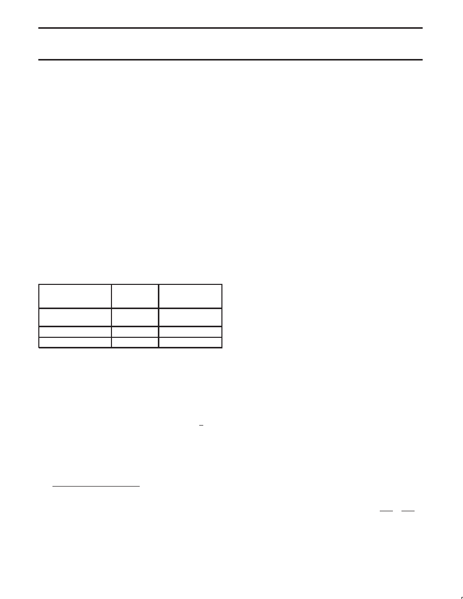
Table 2.
OX2 clock mode bit
(can only be set by
parallel programmer)
X2 bit
(CKCON.0)
CPU clock mode
erased
0
12-clock mode
(default)
erased
1
6-clock mode
programmed
X
6-clock mode
Programmable Clock-Out
A 50% duty cycle clock can be programmed to be output on P1.0.
This pin, besides being a regular I/O pin, has two alternate
functions. It can be programmed:
1. to input the external clock for Timer/Counter 2, or
2. to output a 50% duty cycle clock ranging from 61 Hz to 4 MHz at
a 16 MHz operating frequency in 12-clock mode (122 Hz to
8 MHz in 6-clock mode).
To configure the Timer/Counter 2 as a clock generator, bit C/T2 (in
T2CON) must be cleared and bit T20E in T2MOD must be set. Bit
TR2 (T2CON.2) also must be set to start the timer.
The Clock-Out frequency depends on the oscillator frequency and
the reload value of Timer 2 capture registers (RCAP2H, RCAP2L)
as shown in this equation:
Oscillator Frequency
n
(65536–RCAP2H, RCAP2L)
Where:
n = 2 in 6-clock mode, 4 in 12-clock mode.
(RCAP2H,RCAP2L) = the content of RCAP2H and RCAP2L
taken as a 16-bit unsigned integer.
In the Clock-Out mode Timer 2 roll-overs will not generate an
interrupt. This is similar to when it is used as a baud-rate generator.
It is possible to use Timer 2 as a baud-rate generator and a clock
generator simultaneously. Note, however, that the baud-rate and the
Clock-Out frequency will be the same.
RESET
A reset is accomplished by holding the RST pin HIGH for at least
two machine cycles (24 oscillator periods in 12-clock and 12
oscillator periods in 6-clock mode), while the oscillator is running. To
insure a reliable power-up reset, the RST pin must be high long
enough to allow the oscillator time to start up (normally a few
milliseconds) plus two machine cycles. After the reset, the part runs
in 12-clock mode, unless it has been set to 6-clock operation using a
parallel programmer.
LOW POWER MODES
Stop Clock Mode
The static design enables the clock speed to be reduced down to
0 MHz (stopped). When the oscillator is stopped, the RAM and
Special Function Registers retain their values. This mode allows
step-by-step utilization and permits reduced system power
consumption by lowering the clock frequency down to any value. For
lowest power consumption the Power Down mode is suggested.
Idle Mode
In idle mode (see Table 3), the CPU puts itself to sleep while all of
the on-chip peripherals stay active. The instruction to invoke the idle
mode is the last instruction executed in the normal operating mode
before the idle mode is activated. The CPU contents, the on-chip
RAM, and all of the special function registers remain intact during
this mode. The idle mode can be terminated either by any enabled
interrupt (at which time the process is picked up at the interrupt
service routine and continued), or by a hardware reset which starts
the processor in the same manner as a power-on reset.
Power-Down Mode
To save even more power, a Power Down mode (see Table 3) can
be invoked by software. In this mode, the oscillator is stopped and
the instruction that invoked Power Down is the last instruction
executed. The on-chip RAM and Special Function Registers retain
their values down to 2.0 V and care must be taken to return VCC to
the minimum specified operating voltages before the Power Down
Mode is terminated.
Either a hardware reset or external interrupt can be used to exit from
Power Down. Reset redefines all the SFRs but does not change the
on-chip RAM. An external interrupt allows both the SFRs and the
on-chip RAM to retain their values. WUPD (AUXR1.3–Wakeup from
Power Down) enables or disables the wakeup from power down with
external interrupt. Where:
WUPD = 0: Disable
WUPD = 1: Enable
To properly terminate Power Down, the reset or external interrupt
should not be executed before VCC is restored to its normal
operating level and must be held active long enough for the
oscillator to restart and stabilize (normally less than 10 ms).
To terminate Power Down with an external interrupt, INT0 or INT1
must be enabled and configured as level-sensitive. Holding the pin
low restarts the oscillator but bringing the pin back high completes
the exit. Once the interrupt is serviced, the next instruction to be
executed after RETI will be the one following the instruction that put
the device into Power Down.
相关PDF资料 |
PDF描述 |
|---|---|
| VE-B1B-CU-B1 | CONVERTER MOD DC/DC 95V 200W |
| VE-B14-CU-B1 | CONVERTER MOD DC/DC 48V 200W |
| C8051F557-IM | IC 8051 MCU 16K FLASH 24-QFN |
| MAX4582ESE+T | IC MULTIPLEXER DUAL 4X1 16SOIC |
| MAX4583ESE+T | IC SWITCH TRIPLE SPDT 16SOIC |
相关代理商/技术参数 |
参数描述 |
|---|---|
| P87C591VFA/00,512 | 功能描述:8位微控制器 -MCU 80C51 16K OTP/CAN RoHS:否 制造商:Silicon Labs 核心:8051 处理器系列:C8051F39x 数据总线宽度:8 bit 最大时钟频率:50 MHz 程序存储器大小:16 KB 数据 RAM 大小:1 KB 片上 ADC:Yes 工作电源电压:1.8 V to 3.6 V 工作温度范围:- 40 C to + 105 C 封装 / 箱体:QFN-20 安装风格:SMD/SMT |
| P87C654X2BBD,157 | 功能描述:8位微控制器 -MCU 16K/256 OTP 12/6 CLK I2C LQFP RoHS:否 制造商:Silicon Labs 核心:8051 处理器系列:C8051F39x 数据总线宽度:8 bit 最大时钟频率:50 MHz 程序存储器大小:16 KB 数据 RAM 大小:1 KB 片上 ADC:Yes 工作电源电压:1.8 V to 3.6 V 工作温度范围:- 40 C to + 105 C 封装 / 箱体:QFN-20 安装风格:SMD/SMT |
| P87C654X2FA | 制造商:NXP Semiconductors 功能描述:P87C654X2FA 8bit microcontroller,33MHz |
| P87C654X2FA,529 | 功能描述:8位微控制器 -MCU 16K/256 OTP 12/6 CLK RoHS:否 制造商:Silicon Labs 核心:8051 处理器系列:C8051F39x 数据总线宽度:8 bit 最大时钟频率:50 MHz 程序存储器大小:16 KB 数据 RAM 大小:1 KB 片上 ADC:Yes 工作电源电压:1.8 V to 3.6 V 工作温度范围:- 40 C to + 105 C 封装 / 箱体:QFN-20 安装风格:SMD/SMT |
| P87C654X2FA-S | 功能描述:8位微控制器 -MCU 16K/256 OTP 12/6 CLK I2C PLCC RoHS:否 制造商:Silicon Labs 核心:8051 处理器系列:C8051F39x 数据总线宽度:8 bit 最大时钟频率:50 MHz 程序存储器大小:16 KB 数据 RAM 大小:1 KB 片上 ADC:Yes 工作电源电压:1.8 V to 3.6 V 工作温度范围:- 40 C to + 105 C 封装 / 箱体:QFN-20 安装风格:SMD/SMT |
发布紧急采购,3分钟左右您将得到回复。