- 您现在的位置:买卖IC网 > PDF目录367715 > P87L42 (INTEL CORP) UNIVERSAL PERIPHERAL INTERFACE CHMOS 8-BIT SLAVE MICROCONTROLLER PDF资料下载
参数资料
| 型号: | P87L42 |
| 厂商: | INTEL CORP |
| 元件分类: | 微控制器/微处理器 |
| 英文描述: | UNIVERSAL PERIPHERAL INTERFACE CHMOS 8-BIT SLAVE MICROCONTROLLER |
| 中文描述: | 8-BIT, OTPROM, 0.833 MHz, MICROCONTROLLER, PDIP40 |
| 封装: | PLASTIC, DIP-40 |
| 文件页数: | 6/25页 |
| 文件大小: | 305K |
| 代理商: | P87L42 |
UPI-C42/UPI-L42
If ‘‘EN DMA’’ has been executed, P
27
becomes
the DACK (DMA ACKnowledge) pin. This pin acts
as a chip select input for the Data Bus Buffer
registers during DMA transfers.
EN DMA
Op Code: 0E5H
1
1
1
0
0
1
0
1
D
7
D
0
6.
When EA is enabled on the UPI, the program
counter is placed on Port 1 and the lower four
bits of Port 2 (MSB
e
P
23
, LSB
e
P
10
). On the
UPI this information is multiplexed with PORT
DATA (see port timing diagrams at end of this
data sheet).
7.
The UPI-C42 supports the Quick Pulse Program-
ming Algorithm, but can also be programmed
with the Intelligent Programming Algorithm. (See
the Programming Section.)
UPI-C42 FEATURES
Programmable Memory Size Increase
The user programmable memory on the UPI-C42 will
be increased from the 2K available in the NMOS
product by 2X to 4K. The larger user programmable
memory array will allow the user to develop more
complex peripheral control micro-code. P2.3 (port 2
bit 3) has been designated as the extra address pin
required to support the programming of the extra 2K
of user programmable memory.
The new instruction SEL PMB1 (73h) allows for ac-
cess to the upper 2K bank (locations 2048–4095).
The additional memory is completely transparent to
users not wishing to take advantage of the extra
memory space. No new commands are required to
access the lower 2K bytes. The SEL PMB0 (63h)
has also been added to the UPI-C42 instruction set
to allow for switching between memory banks.
Extended Memory Program
Addressing (Beyond 2K)
For programs of 2K words or less, the UPI-C42 ad-
dresses program memory in the conventional man-
ner. Addresses beyond 2047 can be reached by ex-
ecuting a program memory bank switch instruction
(SEL PMB0, SEL PMB1) followed by a branch in-
struction (JMP or CALL). The bank switch feature
extends the range of branch instructions beyond
their normal 2K range and at the same time prevents
theuserfrominadvertentlycrossingthe2Kboundary.
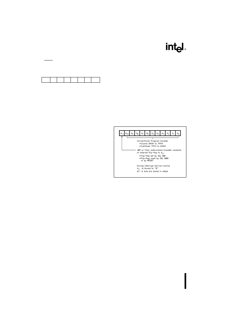
PROGRAM MEMORY BANK SWITCH
The switching of 2K program memory banks is ac-
complished by directly setting or resetting the most
significant bit of the program counter (bit 11); see
Figure 5. Bit 11 is not altered by normal increment-
ing of the program counter, but is loaded with the
contents of a special flip-flop each time a JMP or
CALL instruction is executed. This special flip-flop is
set by executing an SEL PMB1 instruction and reset
by SEL PMB0. Therefore, the SEL PMB instruction
may be executed at any time prior to the actual bank
switch which occurs during the next branch instruc-
tion encountered. Since all twelve bits of the pro-
gram counter, including bit 11, are stored in the
stack, when a Call is executed, the user may jump to
subroutines across the 2K boundary and the proper
PC will be restored upon return. However, the bank
switch flip-flop will not be altered on return.
290414–30
Figure 5. Program Counter
INTERRUPT ROUTINES
Interrupts always vector the program counter to lo-
cation 3 or 7 in the first 2K bank, and bit 11 of the
program counter is held at ‘‘0’’ during the interrupt
service routine. The end of the service routine is sig-
naled by the execution of an RETR instruction. Inter-
rupt service routines should therefore be contained
entirely in the lower 2K words of program memory.
The execution of a SEL PMB0 or SEL PMB1 instruc-
tion within an interrupt routine is not recommended
since it will not alter PC11 while in the routine, but
will change the internal flip-flop.
Hardware A20 Gate Support
This feature has been provided to enhance the per-
formance of the UPI-C42 when being used in a key-
board controller application. The UPI-C42 design
has included on chip logic to support a hardware
GATEA20 feature which eliminates the need to pro-
vide firmware to process A20 command sequences,
6
相关PDF资料 |
PDF描述 |
|---|---|
| P80C42 | UNIVERSAL PERIPHERAL INTERFACE CHMOS 8-BIT SLAVE MICROCONTROLLER |
| P80L42 | UNIVERSAL PERIPHERAL INTERFACE CHMOS 8-BIT SLAVE MICROCONTROLLER |
| P809x-90 | N STR.CLAMP JACK/RG 8, 213,225 RoHS Compliant: Yes |
| P839x-90 | MCS-96 809X-90, 839X-90 |
| P809xBH | RF Coaxial Connector Adapter; Body Material:Brass; Body Plating:Nickel; Body Style:Straight Bulkhead Adapter, Jack-Jack; Contact Material:Beryllium Copper; Contact Plating:Silver; Impedance:50ohm; Series:N; Contact Termination:Crimp RoHS Compliant: Yes |
相关代理商/技术参数 |
参数描述 |
|---|---|
| P87LPC759 | 制造商:PHILIPS 制造商全称:NXP Semiconductors 功能描述:Low power, low price, low pin count (14 pin) microcontroller with 1 kbyte OTP |
| P87LPC759BN | 制造商:PHILIPS 制造商全称:NXP Semiconductors 功能描述:Low power, low price, low pin count (14 pin) microcontroller with 1 kbyte OTP |
| P87LPC760 | 制造商:PHILIPS 制造商全称:NXP Semiconductors 功能描述:Low power, low price, low pin count (14 pin) microcontroller with 1 kbyte OTP |
| P87LPC760BDH | 功能描述:8位微控制器 -MCU 80C51 1K/128 OTP RoHS:否 制造商:Silicon Labs 核心:8051 处理器系列:C8051F39x 数据总线宽度:8 bit 最大时钟频率:50 MHz 程序存储器大小:16 KB 数据 RAM 大小:1 KB 片上 ADC:Yes 工作电源电压:1.8 V to 3.6 V 工作温度范围:- 40 C to + 105 C 封装 / 箱体:QFN-20 安装风格:SMD/SMT |
| P87LPC760BDH,112 | 功能描述:8位微控制器 -MCU 80C51 1K/128 OTP RoHS:否 制造商:Silicon Labs 核心:8051 处理器系列:C8051F39x 数据总线宽度:8 bit 最大时钟频率:50 MHz 程序存储器大小:16 KB 数据 RAM 大小:1 KB 片上 ADC:Yes 工作电源电压:1.8 V to 3.6 V 工作温度范围:- 40 C to + 105 C 封装 / 箱体:QFN-20 安装风格:SMD/SMT |
发布紧急采购,3分钟左右您将得到回复。