- 您现在的位置:买卖IC网 > PDF目录1959 > P89LPC9161FDH,129 (NXP Semiconductors)IC 80C51 MCU FLASH 2KB 16TSSOP PDF资料下载
参数资料
| 型号: | P89LPC9161FDH,129 |
| 厂商: | NXP Semiconductors |
| 文件页数: | 13/27页 |
| 文件大小: | 0K |
| 描述: | IC 80C51 MCU FLASH 2KB 16TSSOP |
| 标准包装: | 96 |
| 系列: | LPC900 |
| 核心处理器: | 8051 |
| 芯体尺寸: | 8-位 |
| 速度: | 18MHz |
| 连通性: | I²C,SPI,UART/USART |
| 外围设备: | 欠压检测/复位,POR,PWM,WDT |
| 输入/输出数: | 14 |
| 程序存储器容量: | 2KB(2K x 8) |
| 程序存储器类型: | 闪存 |
| RAM 容量: | 256 x 8 |
| 电压 - 电源 (Vcc/Vdd): | 2.4 V ~ 3.6 V |
| 数据转换器: | A/D 4x8b; D/A 1x8b |
| 振荡器型: | 内部 |
| 工作温度: | -40°C ~ 85°C |
| 封装/外壳: | 16-TSSOP(0.173",4.40mm 宽) |
| 包装: | 管件 |
| 其它名称: | 935290261129 |
第1页第2页第3页第4页第5页第6页第7页第8页第9页第10页第11页第12页当前第13页第14页第15页第16页第17页第18页第19页第20页第21页第22页第23页第24页第25页第26页第27页
PIC18F87J72 FAMILY
DS39979A-page 78
Preliminary
2010 Microchip Technology Inc.
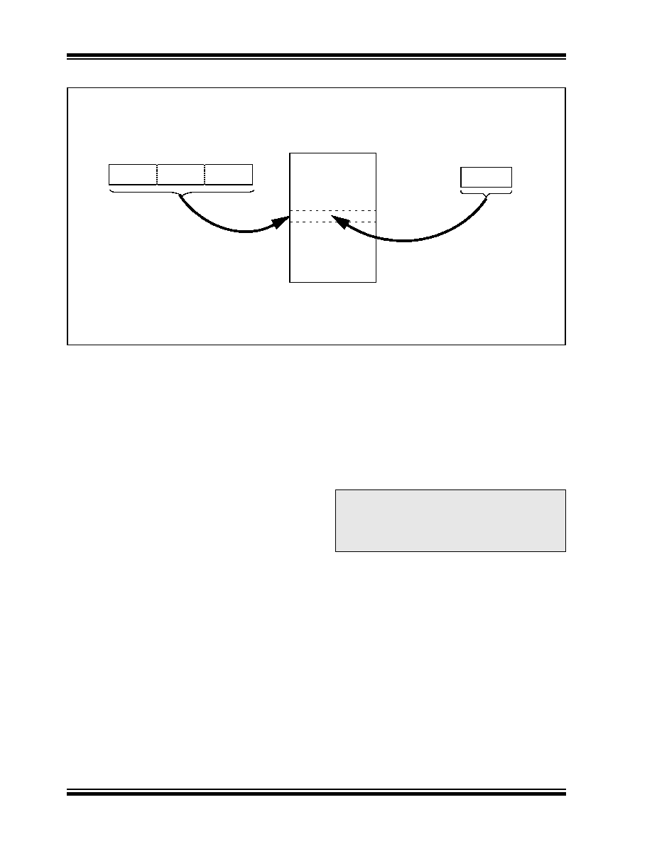
FIGURE 7-2:
TABLE WRITE OPERATION
7.2
Control Registers
Several control registers are used in conjunction with
the TBLRD and TBLWT instructions. These include the:
EECON1 register
EECON2 register
TABLAT register
TBLPTR registers
7.2.1
EECON1 AND EECON2 REGISTERS
The EECON1 register (Register 7-1) is the control
register for memory accesses. The EECON2 register is
not a physical register; it is used exclusively in the
memory write and erase sequences. Reading
EECON2 will read all ‘0’s.
The WPROG bit, when set, allows the user to program
a single word (two bytes) upon the execution of the WR
command. If this bit is cleared, the WR command
programs a block of 64 bytes.
The FREE bit, when set, will allow a program memory
erase operation. When FREE is set, the erase
operation is initiated on the next WR command. When
FREE is clear, only writes are enabled.
The WREN bit, when set, will allow a write operation.
On power-up, the WREN bit is clear. The WRERR bit is
set in hardware when the WR bit is set and cleared
when the internal programming timer expires and the
write operation is complete.
The WR control bit initiates write operations. The bit
cannot be cleared, only set, in software. It is cleared in
hardware at the completion of the write operation.
Table Pointer(1)
Table Latch (8-bit)
TBLPTRH
TBLPTRL
TABLAT
Program Memory
(TBLPTR)
TBLPTRU
Instruction: TBLWT*
Note 1:
Table Pointer actually points to one of 64 holding registers, the address of which is determined by
TBLPTRL<5:0>. The process for physically writing data to the program memory array is discussed in
Holding Registers
Program Memory
Note:
During normal operation, the WRERR is
read as ‘1’. This can indicate that a write
operation was prematurely terminated by
a Reset, or a write operation was
attempted improperly.
相关PDF资料 |
PDF描述 |
|---|---|
| P89LPC917FDH,129 | IC 80C51 MCU FLASH 2K 16-TSSOP |
| P89LPC9221FDH,512 | IC 80C51 MCU FLASH 8K 20-TSSOP |
| P89LPC9321FN,112 | IC 80C51 MCU FLASH 8K 28-DIP |
| P89LPC932A1FA,112 | IC 80C51 MCU FLASH 8K 28-PLCC |
| P89LPC9351FA,112 | IC 80C51 MCU FLASH 8K 28-PLCC |
相关代理商/技术参数 |
参数描述 |
|---|---|
| P89LPC916FDH | 制造商:NXP Semiconductors 功能描述:MCU 8BIT 80C51 2K FLASH TSSOP16 制造商:NXP Semiconductors 功能描述:MCU 8BIT 80C51 2K FLASH, TSSOP16 |
| P89LPC916FDH,118 | 功能描述:8位微控制器 -MCU 2K FL/256B RoHS:否 制造商:Silicon Labs 核心:8051 处理器系列:C8051F39x 数据总线宽度:8 bit 最大时钟频率:50 MHz 程序存储器大小:16 KB 数据 RAM 大小:1 KB 片上 ADC:Yes 工作电源电压:1.8 V to 3.6 V 工作温度范围:- 40 C to + 105 C 封装 / 箱体:QFN-20 安装风格:SMD/SMT |
| P89LPC916FDH,129 | 功能描述:8位微控制器 -MCU ORDER P89LPC916FDH-T T/R RoHS:否 制造商:Silicon Labs 核心:8051 处理器系列:C8051F39x 数据总线宽度:8 bit 最大时钟频率:50 MHz 程序存储器大小:16 KB 数据 RAM 大小:1 KB 片上 ADC:Yes 工作电源电压:1.8 V to 3.6 V 工作温度范围:- 40 C to + 105 C 封装 / 箱体:QFN-20 安装风格:SMD/SMT |
| P89LPC916FDH118 | 制造商:NXP Semiconductors 功能描述:IC 8BIT MCU 80C51 18MHZ TSSOP-16 |
| P89LPC916FDH-S | 功能描述:8位微控制器 -MCU 80C51 2K FL 256B RAM RoHS:否 制造商:Silicon Labs 核心:8051 处理器系列:C8051F39x 数据总线宽度:8 bit 最大时钟频率:50 MHz 程序存储器大小:16 KB 数据 RAM 大小:1 KB 片上 ADC:Yes 工作电源电压:1.8 V to 3.6 V 工作温度范围:- 40 C to + 105 C 封装 / 箱体:QFN-20 安装风格:SMD/SMT |
发布紧急采购,3分钟左右您将得到回复。