- 您现在的位置:买卖IC网 > PDF目录1959 > P89LPC932A1FA,112 (NXP Semiconductors)IC 80C51 MCU FLASH 8K 28-PLCC PDF资料下载
参数资料
| 型号: | P89LPC932A1FA,112 |
| 厂商: | NXP Semiconductors |
| 文件页数: | 29/64页 |
| 文件大小: | 0K |
| 描述: | IC 80C51 MCU FLASH 8K 28-PLCC |
| 产品培训模块: | Migrating from 8/16-Bit MCUs to 32-Bit ARMs |
| 标准包装: | 37 |
| 系列: | LPC900 |
| 核心处理器: | 8051 |
| 芯体尺寸: | 8-位 |
| 速度: | 18MHz |
| 连通性: | I²C,SPI,UART/USART |
| 外围设备: | 欠压检测/复位,LED,POR,PWM,WDT |
| 输入/输出数: | 26 |
| 程序存储器容量: | 8KB(8K x 8) |
| 程序存储器类型: | 闪存 |
| RAM 容量: | 768 x 8 |
| 电压 - 电源 (Vcc/Vdd): | 2.4 V ~ 3.6 V |
| 振荡器型: | 内部 |
| 工作温度: | -40°C ~ 85°C |
| 封装/外壳: | 28-PLCC |
| 包装: | 管件 |
| 产品目录页面: | 706 (CN2011-ZH PDF) |
| 配用: | DB-TSSOP-LPC932-ND - BOARD FOR LPC932 TSSOP 622-1014-ND - BOARD FOR LPC9XX TSSOP 622-1008-ND - BOARD FOR LPC9103 10-HVSON 622-1006-ND - SOCKET ADAPTER BOARD 568-4000-ND - DEMO BOARD SPI/I2C TO DUAL UART 568-3510-ND - DEMO BOARD SPI/I2C TO UART 622-1003-ND - KIT FOR LCD DEMO 622-1002-ND - USB IN-CIRCUIT PROG LPC9XX 568-1759-ND - EMULATOR DEBUGGER/PROGRMMR LPC9X 568-1758-ND - BOARD EVAL FOR LPC93X MCU FAMILY |
| 其它名称: | 568-4279-5 935276131112 P89LPC932A1FA |
第1页第2页第3页第4页第5页第6页第7页第8页第9页第10页第11页第12页第13页第14页第15页第16页第17页第18页第19页第20页第21页第22页第23页第24页第25页第26页第27页第28页当前第29页第30页第31页第32页第33页第34页第35页第36页第37页第38页第39页第40页第41页第42页第43页第44页第45页第46页第47页第48页第49页第50页第51页第52页第53页第54页第55页第56页第57页第58页第59页第60页第61页第62页第63页第64页
P89LPC932A1_3
NXP B.V. 2007. All rights reserved.
Product data sheet
Rev. 03 — 12 March 2007
35 of 64
NXP Semiconductors
P89LPC932A1
8-bit microcontroller with accelerated two-clock 80C51 core
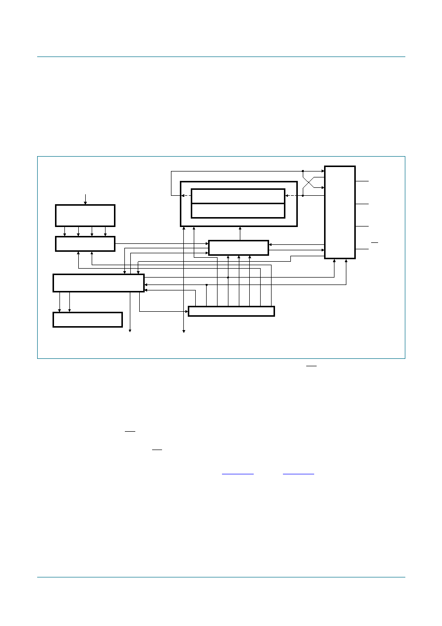
7.22 Serial Peripheral Interface (SPI)
The P89LPC932A1 provides another high-speed serial communication interface—the SPI
interface. SPI is a full-duplex, high-speed, synchronous communication bus with two
operation modes: Master mode and Slave mode. Up to 3 Mbit/s can be supported in
Master mode or up to 2 Mbit/s in Slave mode. It has a Transfer Completion Flag and Write
Collision Flag Protection.
The SPI interface has four pins: SPICLK, MOSI, MISO and SS:
SPICLK, MOSI and MISO are typically tied together between two or more SPI
devices. Data ows from master to slave on MOSI (Master Out Slave In) pin and ows
from slave to master on MISO (Master In Slave Out) pin. The SPICLK signal is output
in the master mode and is input in the slave mode. If the SPI system is disabled, i.e.,
SPEN (SPCTL.6) = 0 (reset value), these pins are congured for port functions.
SS is the optional slave select pin. In a typical conguration, an SPI master asserts
one of its port pins to select one SPI device as the current slave. An SPI slave device
uses its SS pin to determine whether it is selected.
Typical connections are shown in Figure 17 through Figure 19.
Fig 16. SPI block diagram
002aaa900
CPU clock
DIVIDER
BY 4, 16, 64, 128
SELECT
CLOCK LOGIC
SPI CONTROL REGISTER
READ DATA BUFFER
8-BIT SHIFT REGISTER
SPI CONTROL
SPI STATUS REGISTER
SPR1
SPIF
WCOL
SPR0
SPI clock (master)
PIN
CONTROL
LOGIC
S
M
S
M
S
MISO
P2.3
MOSI
P2.2
SPICLK
P2.5
SS
P2.4
SPI
interrupt
request
internal
data
bus
SSIG
SPEN
MSTR
DORD
MSTR
CPHA
CPOL
SPR1
SPR0
MSTR
SPEN
clock
相关PDF资料 |
PDF描述 |
|---|---|
| P89LPC9351FA,112 | IC 80C51 MCU FLASH 8K 28-PLCC |
| P89LPC936FDH,518 | IC 80C51 MCU FLASH 16K 28TSSOP |
| P89LPC938FDH,529 | IC 80C51 MCU FLASH 8K 28-TSSOP |
| P89LPC9401FBD,557 | IC 80C51 MCU FLASH 8K 64-LQFP |
| P89LPC9402FBD,557 | IC 80C51 MCU FLASH 8K 64-LQFP |
相关代理商/技术参数 |
参数描述 |
|---|---|
| P89LPC932A1FDH | 制造商:PHILIPS 制造商全称:NXP Semiconductors 功能描述:8-bit microcontroller with accelerated two-clock 80C51 core 8 kB 3 V byte-erasable flash with 512-byte data EEPROM |
| P89LPC932A1FDH,512 | 功能描述:8位微控制器 -MCU 80C51 8K FL 768B RAM RoHS:否 制造商:Silicon Labs 核心:8051 处理器系列:C8051F39x 数据总线宽度:8 bit 最大时钟频率:50 MHz 程序存储器大小:16 KB 数据 RAM 大小:1 KB 片上 ADC:Yes 工作电源电压:1.8 V to 3.6 V 工作温度范围:- 40 C to + 105 C 封装 / 箱体:QFN-20 安装风格:SMD/SMT |
| P89LPC932A1FDH,529 | 功能描述:8位微控制器 -MCU 8K FL/768B RAM/512B EE/CCU RoHS:否 制造商:Silicon Labs 核心:8051 处理器系列:C8051F39x 数据总线宽度:8 bit 最大时钟频率:50 MHz 程序存储器大小:16 KB 数据 RAM 大小:1 KB 片上 ADC:Yes 工作电源电压:1.8 V to 3.6 V 工作温度范围:- 40 C to + 105 C 封装 / 箱体:QFN-20 安装风格:SMD/SMT |
| P89LPC932A1FDH512 | 制造商:NXP Semiconductors 功能描述:IC 8BIT MCU 80C51 18MHZ TSSOP-28 |
| P89LPC932A1FHN | 制造商:NXP Semiconductors 功能描述:MCU 8BIT 80C51 8K FLASH HVQFN-28 |
发布紧急采购,3分钟左右您将得到回复。