- 您现在的位置:买卖IC网 > PDF目录367747 > PA04 (Electronic Theatre Controls, Inc.) POWER OPERATIONAL AMPLIFIERS PDF资料下载
参数资料
| 型号: | PA04 |
| 厂商: | Electronic Theatre Controls, Inc. |
| 元件分类: | 运算放大器 |
| 英文描述: | POWER OPERATIONAL AMPLIFIERS |
| 中文描述: | 功耗运算放大器 |
| 文件页数: | 4/4页 |
| 文件大小: | 60K |
| 代理商: | PA04 |
OPERATING
CONSIDERATIONS
PA04 PA04A
GENERAL
Please read the “General Operating Considerations” sec-
tion, which covers stability, supplies, heatsinking, mounting,
current limit, SOA interpretation, and specification interpreta-
tion. Additional information can be found in the application
notes. For information on the package outline, heatsinks, and
mounting hardware, consult the “Accessory and Package
Mechanical Data” section of the handbook. The EK04 Evalu-
ation Kit makes prototype circuits a snap by providing an
EK04PC proto circuit board, MS05 mating socket, HS11
heatsink and hardware kit.
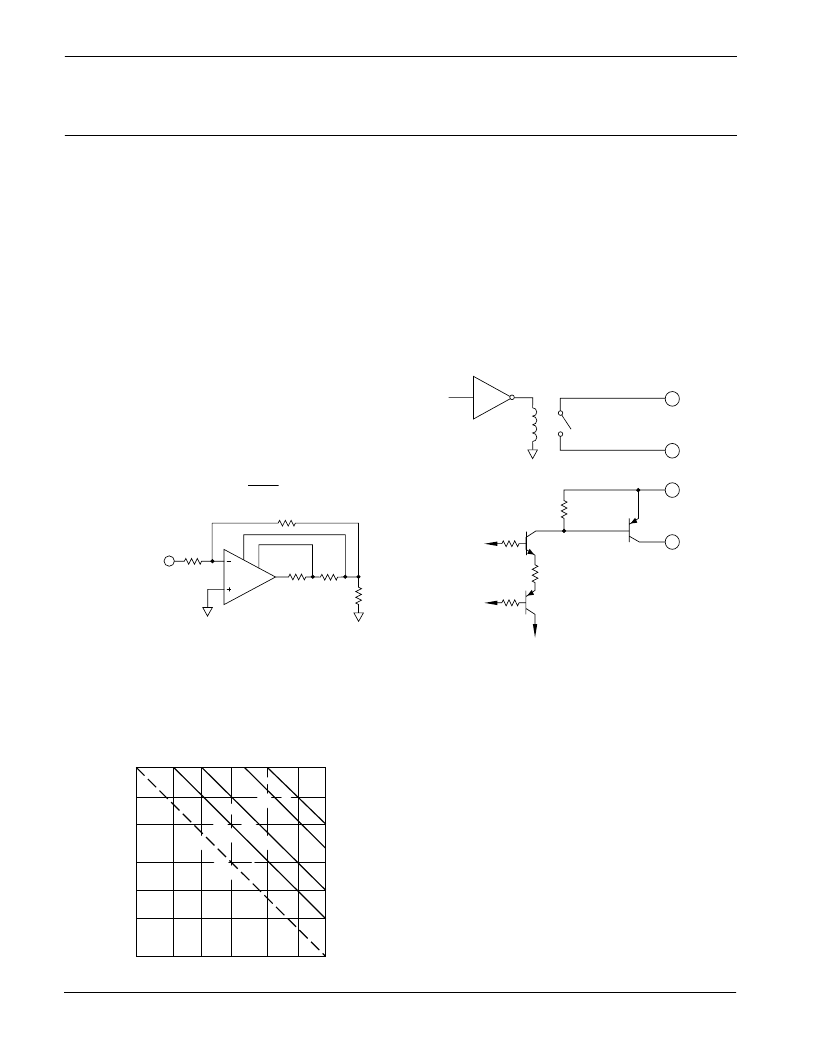
CURRENT LIMIT
The two current limit sense lines are to be connected directly
across the current limit sense resistor.
For the current limit to
work correctly pin 11 must be connected to the amplifier
output side and pin 10 connected to the load side of the
current limit resistor, R
, as shown in Figure 1.
This
connection will bypass any parasitic resistances, Rp, formed
by sockets and solder joints as well as internal amplifier losses.
The current limiting resistor may not be placed anywhere in the
output circuit except where shown in Figure 1.
The value of the current limit resistor can be calculated as
follows:
.76
R
=
I
LIMIT
SAFE OPERATING AREA (SOA)
The MOSFET output stage of this power operational ampli-
fier has two distinct limitations:
1. The current handling capability of the MOSFET geometry
and the wire bonds.
2. The junction temperature of the output MOSFETs.
NOTE:
The output stage is protected against transient flyback.
However, for protection against sustained, high energy
flyback, external fast-recovery diodes should be used.
SLEEP MODE OPERATION
In the sleep mode, pin 12 (sleep) is tied to pin 9 (+V
).
This disables the amplifier’s internal reference and the ampli-
fier shuts down except for a trickle current of 3 mA which flows
into pin 12. Pin 12 should be left open if the sleep mode is not
required.
Several possible circuits can be built to take advantage of
this mode. In Figure 2A a small signal relay is driven by a logic
gate. This removes the requirement to deal with the common
mode voltage that exists on the shutoff circuitry since the sleep
mode is referenced to the +V
voltage.
In Figure 2B, circuitry is used to level translate the sleep
mode input signal. The differential input activates sleep mode
with a differential logic level signal and allows common mode
voltages to
±
V
BOOST
.
BOOST OPERATION
With the V
feature the small signal stages of the
amplifier are operated at higher supply voltages than the
amplifier’s high current output stage. +V
(pin 9) and
–V
(pin 5) are connected to the small signal circuitry of the
amplifier. +V
(pin 8) and –V
(pin 6) are connected to the high
current output stage. An additional 5V on the V
pins is
sufficient to allow the small signal stages to drive the output
transistors into saturation and improve the output voltage
swing for extra efficient operation when required. When close
swings to the supply rails is not required the +V
BOOST
and +V
S
pins must be strapped together as well as the –V
and –V
S
pins. The boost voltage pins must not be at a voltage lower than
the V
S
pins.
COMPENSATION
The external compensation components C
and R
are
connected to pins 3 and 4. Unity gain stability can be achieved
at any compensation capacitance greater than 330 pF with at
least 60 degrees of phase margin. At higher gains more phase
shift can be tolerated in most designs and the compensation
capacitance can accordingly be reduced, resulting in higher
bandwidth and slew rate. Use the typical operating curves as
a guide to select C
C
and R
C
for the application.
Figure 2A. Sleep mode circuit.
LOGIC
K1
9
12
9
12
+V
BOOST
SLEEP
+V
BOOST
SLEEP
560
470
Q1
1K
Q2
–V
BOOST
470
LOGIC
INPUT
+
-
Figure 2B.
Sleep mode circuit.
R
f
R
i
1
2
10
11
R
CL
PA04
R
P
R
L
CL
CL
INPUT
7
Figure 1.
Current Limit.
5.0
2.0
.5
.2
2
SUPPLY TO OUTPUT DIFFERENTIAL (V)
O
5
10
20
50
200
20
DC Tc=125C
DC Tc=85C
DC Tc=25C
t=10m
10
100
1.0
This data sheet has been carefully checked and is believed to be reliable, however, no responsibility is assumed for possible inaccuracies or omissions. All specifications are subject to change without notice.
PA04U REV. I DECEMBER 1997
1997 Apex Microtechnology Corp.
相关PDF资料 |
PDF描述 |
|---|---|
| PA04A | POWER OPERATIONAL AMPLIFIERS |
| PA05A | Voltage-Feedback Operational Amplifier |
| PA05 | Voltage-Feedback Operational Amplifier |
| PA06REMOTEKEYPAD | KEYPAD REMOTE |
| PA07M | Voltage-Feedback Operational Amplifier |
相关代理商/技术参数 |
参数描述 |
|---|---|
| PA-0400 | 制造商:Alltrade Tools LLC 功能描述:EXT.CIRCLIP PLIER DIN A1 |
| PA-0401 | 制造商:Alltrade Tools LLC 功能描述:EXT.CIRCLIP PLIER DIN A2 |
| PA040XS1 | 制造商:AZDISPLAYS 制造商全称:AZ Displays 功能描述:This technical specification applies to 4inch color TFT-LCD module, PA040XS1 |
| PA0423 | 制造商:Pulse 功能描述:PWR TX 8:4 1500VDC SGL+AUX PRIM. SGL SEC. 48V PRIM. 12V SEC. - Bulk |
| PA0423NL | 制造商:Pulse 功能描述:- Trays |
发布紧急采购,3分钟左右您将得到回复。