- 您现在的位置:买卖IC网 > PDF目录296790 > PBA31301/3S (INFINEON TECHNOLOGIES AG) SPECIALTY TELECOM CIRCUIT, PBGA34 PDF资料下载
参数资料
| 型号: | PBA31301/3S |
| 厂商: | INFINEON TECHNOLOGIES AG |
| 元件分类: | 通信及网络 |
| 英文描述: | SPECIALTY TELECOM CIRCUIT, PBGA34 |
| 封装: | 10.20 X 14 MM, 1.60 MM HEIGHT, SOBGA-34 |
| 文件页数: | 9/12页 |
| 文件大小: | 812K |
| 代理商: | PBA31301/3S |
6
PBA 313 01
EN/LZT 146 65 R3B Ericsson Microelectronics AB, October 2001
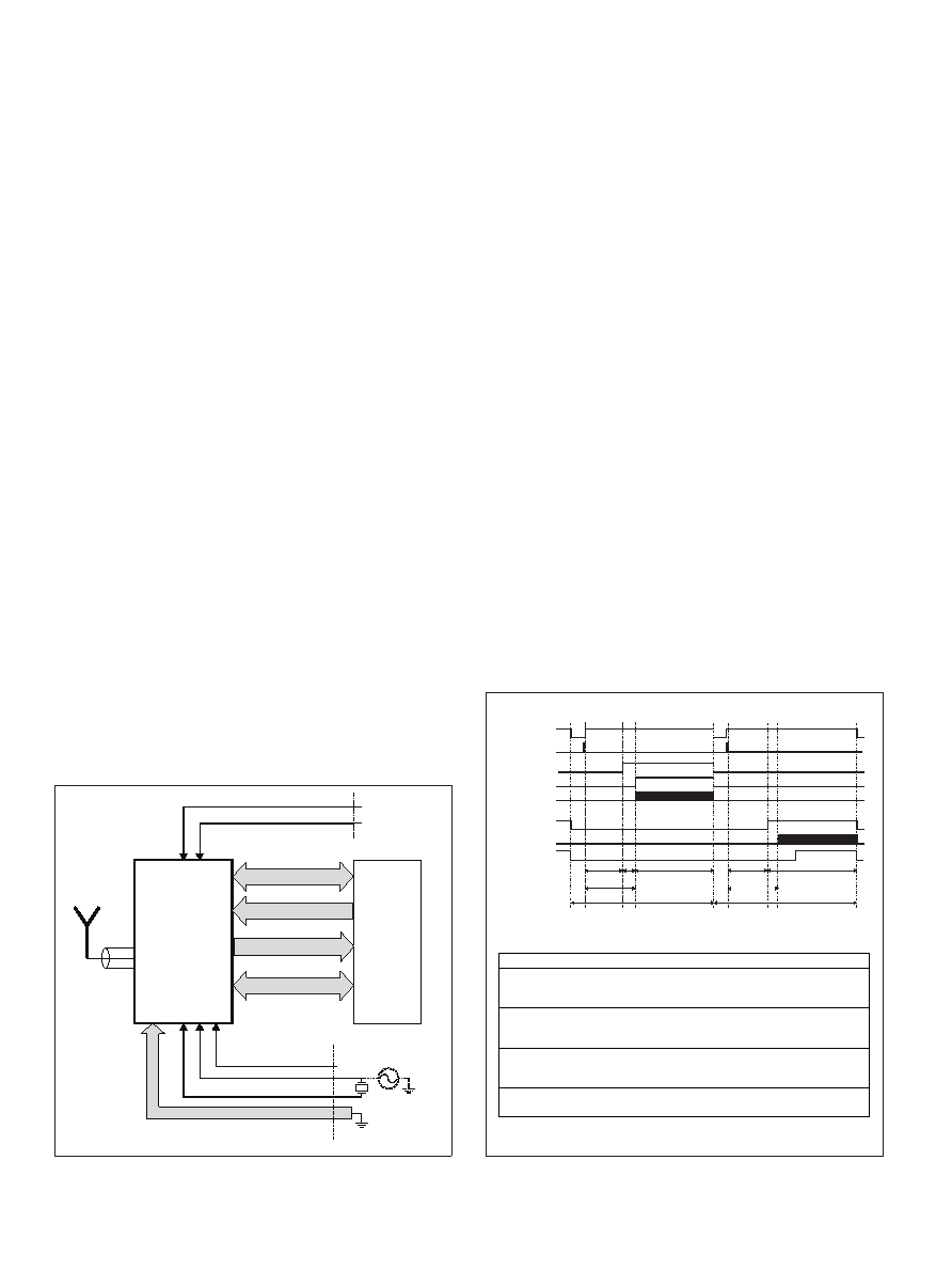
I/O Signal Description
Power supply
There are two connections to supply the Bluetooth radio with
power. VCC_VCO supplies the sensitive VCO circuitry with
power, and VCC is for the remaining circuitry. Each of the two
supplies should be low frequency decoupled. See figure 13
for example circuitry.
Oscillator or external clock input
Refer to the Design Considerations section.
Oscillator or external clock input XO_N and XO_P connects to
the crystal's inputs. The load capacitance to the crystal can
be trimmed using the XO-Trim register. If an external clock is
used, it should be AC coupled into the XO_N input and the
XO_P input shall be left unconnected.
Antenna
The ANT pin should be connected to a 50 antenna interface,
thereby supporting the best signal strength performance.
Ericsson Microelectronics' partners can support application
specific antennas.
Input Control
There are six digital inputs available for controlling the radio
features of the PBA 313 01. The Bluetooth timing require-
ments for these are decribed in figure 6. In addition, there is
a digital input signal for hardware reset of the radio, and a
digital input signal for waking up the clock circuitry after a
sleep mode period.
SYNT_ON
Synthesizer on control is active 'high'. Activate this signal to
power up of the VCO section of the radio. SYNT_ON is used
in both transmit and receive mode.
RX_ON
Receive-on control is active 'high'. Activate this signal to
enable reception of Bluetooth data on the RX_DATA pin. The
transmit-on control (TX_ON) must be deactivated and the
synthesiser (SYNT_ON) activated if data is to be received.
PX_ON
Packet switch on control is active 'high'. Activate this signal
during reception of a Bluetooth payload.
PX_ON is used to control the Dynamic Automatic Frequency
Compensation (DAFC) of the receiver. Since the General
Inquiry Access Code (GIAC), information in a Bluetooth
packet header contains an equal number of one's (+FMOD)
and zero's (-FMOD), the average frequency will always be
centered on the carrier frequency. This provides the DAFC
with the reference for the fast tuning. If the fast mode is not
used during the header then the first bits could be interpreted
incorrectly.
The slow mode gives a more accurate FSK compensation
of the thresholds for a one and a zero compared to the
fast mode; therefore, the BER is less. The fast mode (time
constant <2s) is used when PX_ON is deactived and the
slow mode (time constant <50s) when it is activated.
TX_ON
Transmit-on control is active 'high'. Activate this signal to
enable radio signal output on the ANT pin. The actual transfer
of data that exists on the TX_DATA input occurs when
PHD_OFF goes 'high'. The receive-on control, RX_ON, must
also be 'low' if data is to be transmitted.
GROUND
ANTENNA
PBA 313 01
Base-
band
CLOCK 13 MHz
VCC_VCO
VCC
Input control
11 PINS
4 PINS
6 PINS
4 PINS
POR_EXT
XO_N
XO_P
Serial interface
Output control
4 PINS
Data interface
Figure 5. System overview.
Symbol Parameter
Min
Typical
Max
Unit
tS
One Slot time
625
s
tS
Two Slot times
1875
s
tS
Three Slot times
3125
s
tTO
Transmitter On delay
102
s
tTD
Delay before transmitting data
203
213
223
s
tPHD
Phase Detector Off delay after tTO
104
s
tD
Data sending period, one slot
366
s
tD
Data sending period, two slots
1598
s
tD
Data sending period, three slots
2862
s
tRO
Receiver On delay
175
213
s
tRD
Delay before receiving data
213
s
TX SLOT
SYNT_ON
TX_ON
PHD_OFF
TX_DATA
RX_ON
SI_CDI
RX_DATA
PHD
t
D
t
S
t
TO
t
TD
t
RD
t
RO
t
D
t
S
t
RX SLOT
PX_ON
Figure 6 and table 2. Timing sequence for data transmission.
相关PDF资料 |
PDF描述 |
|---|---|
| PBA31301/3S | SPECIALTY TELECOM CIRCUIT, CBGA34 |
| PBL38773/1ML | TELECOM-SLIC, PQCC32 |
| PBL38773/1SO | TELECOM-SLIC, PDSO28 |
| PC-PVC-271K | 1 ELEMENT, 270 uH, GENERAL PURPOSE INDUCTOR |
| PC-PVC-270K | 1 ELEMENT, 27 uH, GENERAL PURPOSE INDUCTOR |
相关代理商/技术参数 |
参数描述 |
|---|---|
| PBA31302 | 制造商:INFINEON 制造商全称:Infineon Technologies AG 功能描述:Bluetooth Radio Transceiver |
| PBA31304 | 制造商:未知厂家 制造商全称:未知厂家 功能描述:Telecomm/Datacomm |
| PBA31305 | 制造商:INFINEON 制造商全称:Infineon Technologies AG 功能描述:Bluetooth Radio Transceiver |
| PBA31307 | 制造商:INFINEON 制造商全称:Infineon Technologies AG 功能描述:SINGLE STONE |
| PBA31307/1R2AT | 功能描述:MODULE BLUETOOTH SINGLESTONE RoHS:否 类别:RF/IF 和 RFID >> RF 收发器 系列:- 产品培训模块:Lead (SnPb) Finish for COTS Obsolescence Mitigation Program 标准包装:30 系列:- 频率:4.9GHz ~ 5.9GHz 数据传输率 - 最大:54Mbps 调制或协议:* 应用:* 功率 - 输出:-3dBm 灵敏度:- 电源电压:2.7 V ~ 3.6 V 电流 - 接收:* 电流 - 传输:* 数据接口:PCB,表面贴装 存储容量:- 天线连接器:PCB,表面贴装 工作温度:-25°C ~ 85°C 封装/外壳:68-TQFN 裸露焊盘 包装:管件 |
发布紧急采购,3分钟左右您将得到回复。