- 您现在的位置:买卖IC网 > PDF目录378041 > PBL386402QNS (ERICSSON) Subscriber Line Interface Circuit PDF资料下载
参数资料
| 型号: | PBL386402QNS |
| 厂商: | ERICSSON |
| 英文描述: | Subscriber Line Interface Circuit |
| 中文描述: | 用户线接口电路 |
| 文件页数: | 15/16页 |
| 文件大小: | 138K |
| 代理商: | PBL386402QNS |
PBL 386 40/2
15
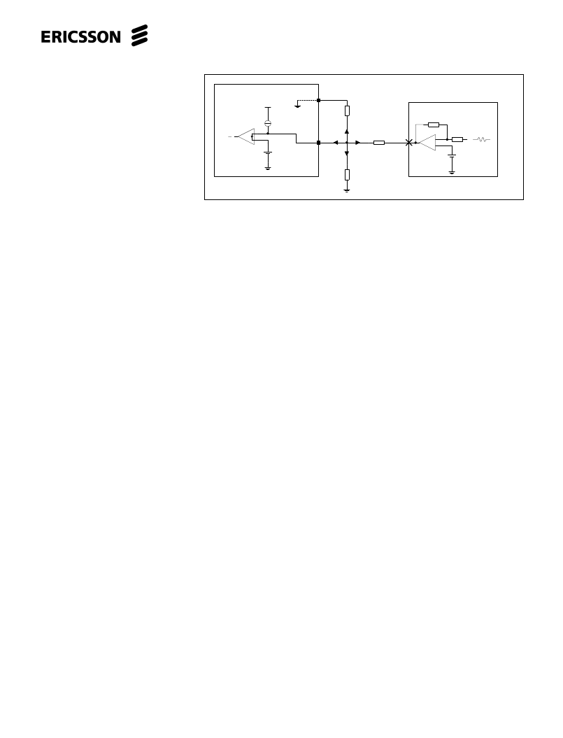
Figure 14. CODEC receive interface.
PBL386 40/2
CODEC
+
_
VTX
RSN
R
RX
R
T
R
R
I
RRX
I
RSN
I
RT
I
RR
U
REFcodec
+1.25 V
I
DC-GND
trip detection network. This network is
applicable, when the ring voltage super-
imposed on V
and is injected on the ring
lead of the two-wire port. The dc voltage
across sense resistor R
is monitored by
the ring trip comparator input DT and DR
via the network R
, R
, R
, R
, C
and C
2
.
With the line on-hook (no dc current) DT
is more positive than DR and the DET
output will report logic level high, i.e. the
detector is not tripped. When the line
goes off-hook, while ringing, a dc current
will flow through the loop including sense
resistor R
and will cause input DT to
become more negative than input DR.
This changes output DET to logic level
low, i.e. tripped detector condition. The
system controller (or line card processor)
responds by de-energizing the ring relay,
i.e. ring trip.
Complete filtering of the 20 Hz ac
component at terminal DT and DR is not
necessary. A toggling DET output can be
examined by a software routine to deter-
mine the duty cycle. When the DET
output is at logic level low for more than
half the time, off-hook condition is
indicated.
Relay driver
The PBL 386 40/2 SLIC incorporates a
ring relay driver designed as open
collector (npn) with a current sinking
capability of 50 mA. The drive transistor
emitter is connected to BGND. The relay
driver has an internal zener diode clamp
for inductive kick-back voltages.
Care must be taken when using the relay
driver together with relays that have high
impedance.
Control Inputs
The PBL 386 40/2 SLIC have three
digital control inputs, C1, C2 and C3.
A decoder in the SLIC interprets the
control input condition and sets up the
commanded operating state.
C1 to C3 are internal pull-up inputs.
Open Circuit State
In the Open Circuit State the TIPX and
RINGX line drive amplifiers as well as
other circuit blocks are powered down.
This causes the SLIC to present a high
impedance to the line. Power dissipation
is at a minimum and no detectors are
active.
Ringing State
The ring relay driver and the ring trip
detector are activated and the ring trip
detector is indicating off hook with a logic
low level at the detector output.
The SLIC is in the active normal state.
Active States
TIPX is the terminal closest to ground
and sources loop current while RINGX is
the more negative terminal and sinks
loop current. Vf signal transmission is
normal. The loop current or the ground
key detector is activated. The loop
current detector is indicating off hook
with a logic low level and the ground key
detector is indicating active ground key
with a logic high level present at the
detector output.
In PBL 386 40/2 a line voltage meas-
urement feature is available in the active
state, which may be used for line length
estimations or for line test purposes. The
line voltage is presented on the detector
output as a pulse at logic high level with
a pulsewidth of 5.5
μ
s/V. To start the line
voltage measurement this mode has to
be entered from the Active State with the
loop or ground key detector active. The
pulse presented at the DET output
proportional to the line voltage starts
when entering the line voltage measuring
mode.
Tip Open State
Tip Open State is used for ground start
signalling.
In this state the SLICs present a high
impedance to the line on the TIPX pin
and the programmed dc characteristic,
with the longitudinal current compensa-
tion (see section Longitudinal Imped-
ance) not active, to the line on the
RINGX pin.
The loop current detector is active.
Active Polarity Reversal State
TIPX and RINGX polarity is reversed
from the Active State: RINGX is the
terminal closest to ground and sources
loop current while TIPX is the more
negative terminal and sinks current. Vf
signal transmission is normal. The loop
current or the ground key detector is
activated. The loop current detector is
indicating off hook with a logic low level
and the ground key detector is indicating
active ground key with a logic high level
present at the detector output.
Overvoltage Protection
The PBL 386 40/2 SLIC must be pro-
tected against overvoltages on the
telephone line caused by lightning, ac
power contact and induction. Refer to
Maximum Ratings, TIPX and RINGX
terminals, for maximum allowable
continuous and transient ratings that
may be applied to the SLIC.
Secondary Protection
The circuit shown in figure 12 utilizes
series resistors together with a program-
mable overvoltage protector
(e.g. PowerInnovations TISPPBL2),
serving as a secondary protection.
The TISP PBL2 is a dual forward-
conducting buffered p-gate overvoltage
protector. The protector gate references
the protection (clamping) voltage to
negative supply voltage (i e the battery
voltage, V
). As the protection voltage
will track the negative supply voltage the
overvoltage stress on the SLIC is
minimized.
Positive overvoltages are clamped to
ground by a diode. Negative overvolt-
ages are initially clamped close to the
SLIC negative supply rail voltage and the
相关PDF资料 |
PDF描述 |
|---|---|
| PBL386502 | Subscriber Line Interface Circuit |
| PBL386502QNS | Subscriber Line Interface Circuit |
| PBL386502QNT | Subscriber Line Interface Circuit |
| PBL38650-2 | TERMINAL |
| PBL386502SHT | Subscriber Line Interface Circuit |
相关代理商/技术参数 |
参数描述 |
|---|---|
| PBL386402QNT | 制造商:ERICSSON 制造商全称:Ericsson 功能描述:Subscriber Line Interface Circuit |
| PBL386402QNTNT | 制造商:Infineon Technologies AG 功能描述:SLIC 1-CH 66dB 45mA 5V/-9V/-12V/-15V/-18V/-24V/-28V 28-Pin PLCC T/R |
| PBL386402SHT | 制造商:ERICSSON 制造商全称:Ericsson 功能描述:Subscriber Line Interface Circuit |
| PBL386402SOAXT | 制造商:Lantiq 功能描述:SLIC 1-CH 66dB 45mA 5V/-9V/-12V/-15V/-18V/-24V/-28V 24-Pin DSO T/R |
| PBL386402SOS | 制造商:ERICSSON 制造商全称:Ericsson 功能描述:Subscriber Line Interface Circuit |
发布紧急采购,3分钟左右您将得到回复。