参数资料
| 型号: | PCA9535ECDTR2G |
| 厂商: | ON Semiconductor |
| 文件页数: | 7/20页 |
| 文件大小: | 0K |
| 描述: | 16-BIT I/O EXPANDER 24TSSOP |
| 标准包装: | 2,500 |
| 接口: | I²C 总线,SM 总线 |
| 输入/输出数: | 16 |
| 中断输出: | 是 |
| 频率 - 时钟: | 100kHz |
| 电源电压: | 1.65 V ~ 5.5 V |
| 工作温度: | -55°C ~ 125°C |
| 安装类型: | 表面贴装 |
| 封装/外壳: | 24-TSSOP(0.173",4.40mm 宽) |
| 供应商设备封装: | 24-TSSOP |
| 包装: | 带卷 (TR) |
| 包括: | * |
PCA9535E, PCA9535EC
http://onsemi.com
15
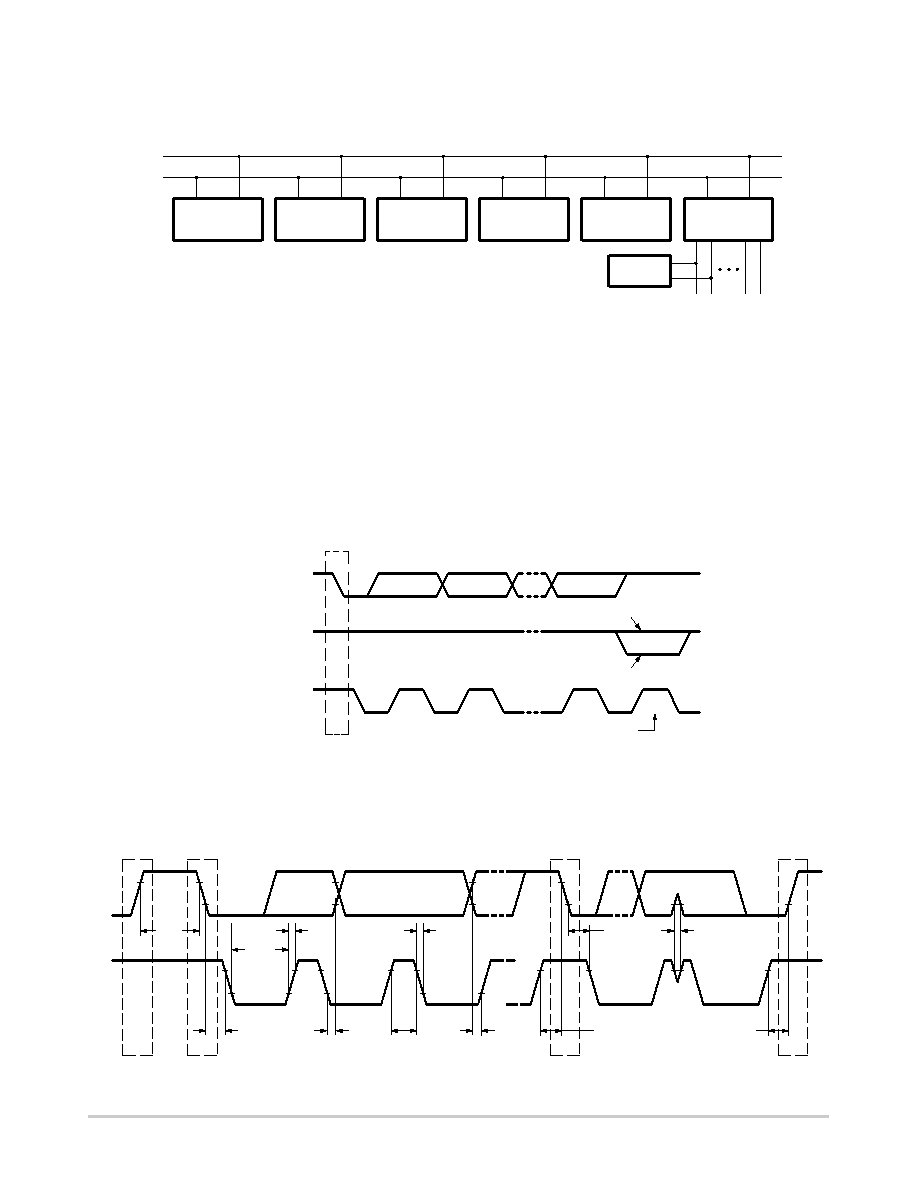
System Configuration
A device generating a message is a ‘transmitter’; a device
receiving is the ‘receiver’. The device that controls the
message is the ‘master’ and the devices which are controlled
by the master are the ‘slaves’ (see Figure 16).
Figure 16. System Configuration
MASTER
TRANSMITTER/
RECEIVER
SLAVE
RECEIVER
SLAVE
TRANSMITTER/
RECEIVER
MASTER
TRANSMITTER
MASTER
TRANSMITTER/
RECEIVER
SDA
SCL
I2CBUS
MULTIPLEXER
SLAVE
Acknowledge
The number of data bytes transferred between the START
and the STOP conditions from transmitter to receiver is not
limited. Each 8bit byte is followed by one acknowledge bit.
The acknowledge bit is a HIGH level put on the bus by the
transmitter, whereas the master generates an extra clock
pulse for the acknowledge bit.
A slave receiver which is addressed must generate an
acknowledge after the reception of each byte. Also a master
must generate an acknowledge after the reception of each
byte that has been clocked out of the slave transmitter. The
device that acknowledges has to pull down the SDA line
during the acknowledge clock pulse, such that the SDA line
is stable LOW during the HIGH period of the acknowledge
clock pulse; setup time and hold time must be taken into
account.
A master receiver signals an end of data to the transmitter
by not generating an acknowledge on the last byte that has
been clocked out of the slave. In this event, the transmitter
must leave the data line HIGH to enable the master to
generate a STOP condition.
Figure 17. Acknowledgement of the I2C Bus
S
START
condition
9
8
2
1
clock pulse for
acknowledgement
not acknowledge
acknowledge
data output
by transmitter
data output
by receiver
SCL from master
Timing and Test Setup
Figure 18. Definition of Timing on the I2C Bus
tSP
tBUF
tHD;STA
P
S
tLOW
tr
tHD;DAT
tf
tHIGH
tSU;DAT
tSU;STA
Sr
tHD;STA
tSU;STO
SDA
SCL
相关PDF资料 |
PDF描述 |
|---|---|
| CAT9555HT6I-GT2 | IC I/O EXPANDER 16BI 2C 24TQFN |
| PCA8574AN,112 | IC I/O EXPANDER I2C 8B 16DIP |
| CAT9555HV6I-GT2 | IC I/O EXPANDER I2C/SMBUS 24TQFN |
| JLC1562BNG | IC I/O EXPANDER I2C 8B 16DIP |
| CAT9555WI-T1 | IC I/O EXPANDER I2C 16B 24SOIC |
相关代理商/技术参数 |
参数描述 |
|---|---|
| PCA9535ECDWR2G | 功能描述:接口-I/O扩展器 16-BIT I/O EXPANDER RoHS:否 制造商:NXP Semiconductors 逻辑系列: 输入/输出端数量: 最大工作频率:100 kHz 工作电源电压:1.65 V to 5.5 V 工作温度范围:- 40 C to + 85 C 安装风格:SMD/SMT 封装 / 箱体:HVQFN-16 封装:Reel |
| PCA9535ECMTTXG | 功能描述:接口-I/O扩展器 16-BIT I/O EXPANDER RoHS:否 制造商:NXP Semiconductors 逻辑系列: 输入/输出端数量: 最大工作频率:100 kHz 工作电源电压:1.65 V to 5.5 V 工作温度范围:- 40 C to + 85 C 安装风格:SMD/SMT 封装 / 箱体:HVQFN-16 封装:Reel |
| PCA9535EDTR2G | 功能描述:接口-I/O扩展器 16-BIT I/O EXPANDER RoHS:否 制造商:NXP Semiconductors 逻辑系列: 输入/输出端数量: 最大工作频率:100 kHz 工作电源电压:1.65 V to 5.5 V 工作温度范围:- 40 C to + 85 C 安装风格:SMD/SMT 封装 / 箱体:HVQFN-16 封装:Reel |
| PCA9535EDWR2G | 功能描述:接口-I/O扩展器 16-BIT I/O EXPANDER RoHS:否 制造商:NXP Semiconductors 逻辑系列: 输入/输出端数量: 最大工作频率:100 kHz 工作电源电压:1.65 V to 5.5 V 工作温度范围:- 40 C to + 85 C 安装风格:SMD/SMT 封装 / 箱体:HVQFN-16 封装:Reel |
| PCA9535EMTTXG | 功能描述:接口-I/O扩展器 16-BIT I/O EXPANDER RoHS:否 制造商:NXP Semiconductors 逻辑系列: 输入/输出端数量: 最大工作频率:100 kHz 工作电源电压:1.65 V to 5.5 V 工作温度范围:- 40 C to + 85 C 安装风格:SMD/SMT 封装 / 箱体:HVQFN-16 封装:Reel |
发布紧急采购,3分钟左右您将得到回复。