参数资料
| 型号: | PCA9655EDTR2G |
| 厂商: | ON Semiconductor |
| 文件页数: | 2/20页 |
| 文件大小: | 0K |
| 描述: | IC I/O EXPANDER I2C 16B 24-TSSOP |
| 标准包装: | 1 |
| 接口: | I²C 总线,SM 总线 |
| 输入/输出数: | 16 |
| 中断输出: | 是 |
| 频率 - 时钟: | 100kHz |
| 电源电压: | 1.65 V ~ 5.5 V |
| 工作温度: | -55°C ~ 125°C |
| 安装类型: | 表面贴装 |
| 封装/外壳: | 24-TSSOP(0.173",4.40mm 宽) |
| 供应商设备封装: | 24-TSSOP |
| 包装: | 标准包装 |
| 其它名称: | PCA9655EDTR2GOSDKR |
PCA9655E
http://onsemi.com
10
Registers 4 and 5: Polarity Inversion Registers
These registers allow the polarity of the data in the input
port registers to be inverted. The input port data polarity will
be inverted when its corresponding bit in these registers is
set (written with ‘1’), and retained when the bit is cleared
(written with a ‘0’).
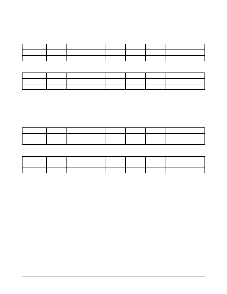
Table 12. POLARITY INVERSION PORT 0 REGISTER
Bit
7
6
5
4
3
2
1
0
Symbol
N0.7
N0.6
N0.5
N0.4
N0.3
N0.2
N0.1
N0.0
Default
0
Table 13. POLARITY INVERSION PORT 1 REGISTER
Bit
7
6
5
4
3
2
1
0
Symbol
N1.7
N1.6
N1.5
N1.4
N1.3
N1.2
N1.1
N1.0
Default
0
Registers 6 and 7: Configuration Registers
The I/O pin directions are configured through the
configuration registers. When a bit in the configuration
registers is set (written with ‘1’), the bit’s corresponding port
pin is enabled as an input with the output driver in
highimpedance. When a bit is cleared (written with ‘0’),
the corresponding port pin is enabled as an output. Note that
there is a high value resistor tied to VDDat each pin. At reset,
the device’s ports are inputs with a pullup to VDD.
Table 14. CONFIGURATION PORT 0 REGISTER
Bit
7
6
5
4
3
2
1
0
Symbol
C0.7
C0.6
C0.5
C0.4
C0.3
C0.2
C0.1
C0.0
Default
1
Table 15. CONFIGURATION PORT 1 REGISTER
Bit
7
6
5
4
3
2
1
0
Symbol
C1.7
C1.6
C1.5
C1.4
C1.3
C1.2
C1.1
C1.0
Default
1
Poweron Reset
Upon application of power, an internal PowerOn Reset
(POR) holds the PCA9655E in a reset condition while VDD
is ramping up. When VDD has reached VPOR, the reset
condition is released and the PCA9655E registers and
SMBus state machine will initialize to their default states.
The reset is typically completed by the POR and the part
enabled by the time the power supply is above VPOR.
However, when doing a power reset cycle, it is necessary to
lower the power supply below 0.2 V, and then restored to the
operating voltage.
I/O Port (see Figure 2)
When an I/O pin is configured as an input, FETs Q1 and
Q2 are off, creating a highimpedance input with a weak
pullup (100 k
W typ) to VDD. The input voltage may be
raised above VDD to a maximum of 5.5 V.
When the I/O pin is configured as an output, then either Q1
or Q2 is enabled, depending on the state of the Output Port
register. Care should be exercised if an external voltage is
applied to an I/O configured as an output because of the
lowimpedance path that exists between the pin and either
VDD or VSS.
相关PDF资料 |
PDF描述 |
|---|---|
| 3448-55 | STRAIN RELIEF 26 POS |
| IS82C55AZ | IC I/O EXPANDER 24B 44PLCC |
| 3448-57 | STRAIN RELIEF 40 POS |
| CS82C55A | IC I/O EXPANDER 24B 44PLCC |
| CQ82C55AZ | IC I/O EXPANDER 24B 44MQFP |
相关代理商/技术参数 |
参数描述 |
|---|---|
| PCA9655EDWR2G | 功能描述:接口-I/O扩展器 16-BIT I/O EXPANDER RoHS:否 制造商:NXP Semiconductors 逻辑系列: 输入/输出端数量: 最大工作频率:100 kHz 工作电源电压:1.65 V to 5.5 V 工作温度范围:- 40 C to + 85 C 安装风格:SMD/SMT 封装 / 箱体:HVQFN-16 封装:Reel |
| PCA9655EMTTXG | 功能描述:接口-I/O扩展器 I2C I/O EXPANDER RoHS:否 制造商:NXP Semiconductors 逻辑系列: 输入/输出端数量: 最大工作频率:100 kHz 工作电源电压:1.65 V to 5.5 V 工作温度范围:- 40 C to + 85 C 安装风格:SMD/SMT 封装 / 箱体:HVQFN-16 封装:Reel |
| PCA9661B,118 | 功能描述:I2C 接口集成电路 PARALLEL BUS TO FM+I2C BUS CONTRLLR RoHS:否 制造商:NXP Semiconductors 电源电压-最大:5.5 V 电源电压-最小:2.3 V 最大工作频率:400 KHz 最大工作温度:+ 85 C 封装 / 箱体:TSSOP-16 |
| PCA9663B,118 | 功能描述:接口-I/O扩展器 7VIN 3.3VOUT 100KHz RoHS:否 制造商:NXP Semiconductors 逻辑系列: 输入/输出端数量: 最大工作频率:100 kHz 工作电源电压:1.65 V to 5.5 V 工作温度范围:- 40 C to + 85 C 安装风格:SMD/SMT 封装 / 箱体:HVQFN-16 封装:Reel |
| PCA9663B118 | 制造商:NXP 功能描述: 制造商:NXP Semiconductors 功能描述: |
发布紧急采购,3分钟左右您将得到回复。