参数资料
| 型号: | PCA9670BS,118 |
| 厂商: | NXP Semiconductors |
| 文件页数: | 31/35页 |
| 文件大小: | 0K |
| 描述: | IC I/O EXPANDER I2C 8B 16HVQFN |
| 标准包装: | 6,000 |
| 接口: | I²C |
| 输入/输出数: | 8 |
| 中断输出: | 无 |
| 频率 - 时钟: | 1MHz |
| 电源电压: | 2.3 V ~ 5.5 V |
| 工作温度: | -40°C ~ 85°C |
| 安装类型: | 表面贴装 |
| 封装/外壳: | 16-VFQFN 裸露焊盘 |
| 供应商设备封装: | 16-HVQFN |
| 包装: | 带卷 (TR) |
| 包括: | POR |
| 其它名称: | 935282714118 PCA9670BS-T PCA9670BS-T-ND |
第1页第2页第3页第4页第5页第6页第7页第8页第9页第10页第11页第12页第13页第14页第15页第16页第17页第18页第19页第20页第21页第22页第23页第24页第25页第26页第27页第28页第29页第30页当前第31页第32页第33页第34页第35页
PCA9670
All information provided in this document is subject to legal disclaimers.
NXP B.V. 2013. All rights reserved.
Product data sheet
Rev. 3 — 30 May 2013
5 of 35
NXP Semiconductors
PCA9670
Remote 8-bit I/O expander for Fm+ I2C-bus with reset
[1]
HVQFN16 package die supply ground is connected to both the VSS pin and the exposed center pad. The
VSS pin must be connected to supply ground for proper device operation. For enhanced thermal, electrical,
and board-level performance, the exposed pad needs to be soldered to the board using a corresponding
thermal pad on the board, and for proper heat conduction through the board thermal vias need to be
incorporated in the PCB in the thermal pad region.
7.
Functional description
Refer to Figure 1 “Block diagram of PCA9670”.
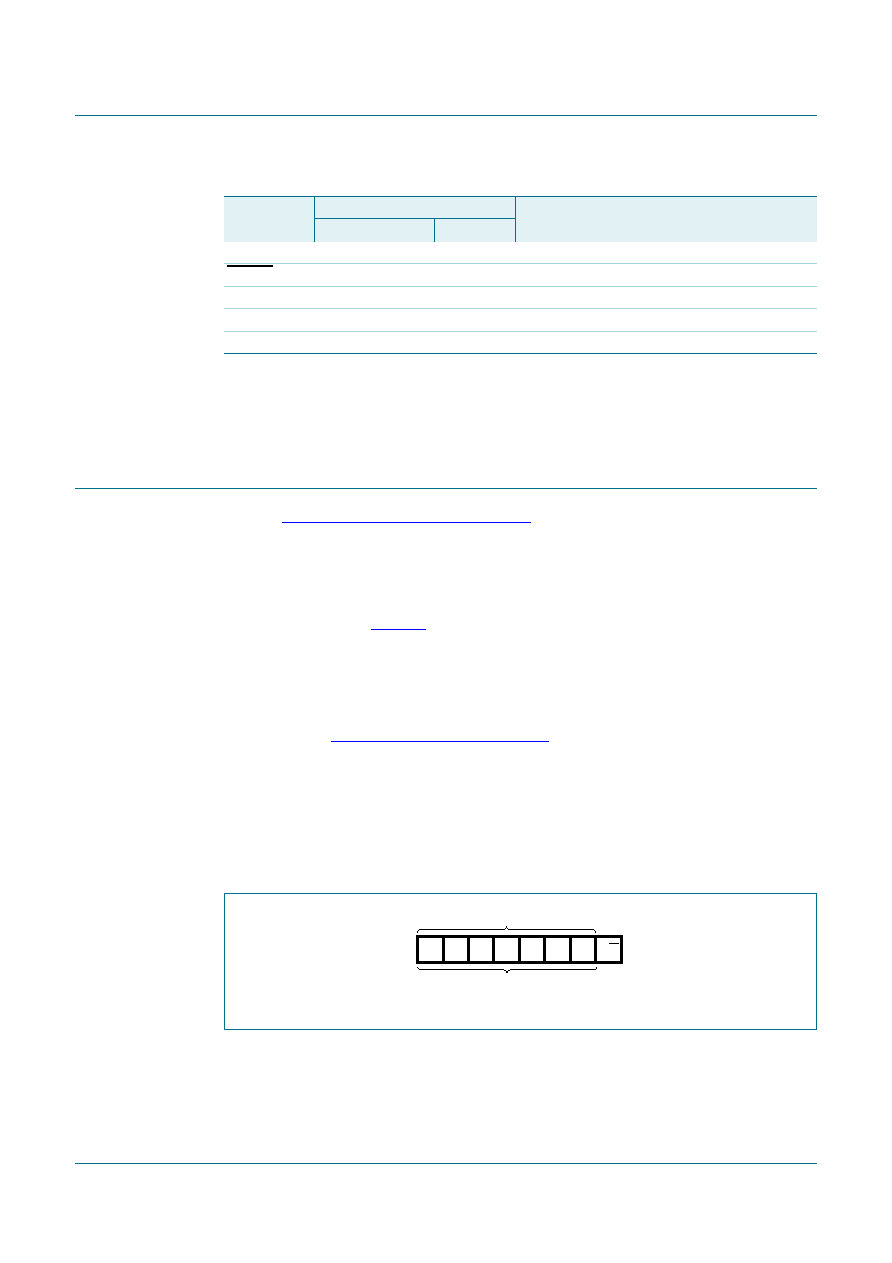
7.1 Device address
Following a START condition, the bus master must send the address of the slave it is
accessing and the operation it wants to perform (read or write). The address format of the
PCA9670 is shown in Figure 6. Slave address pins AD2, AD1, and AD0 are used to
choose one of 64 slave addresses. These devices can monitor the change in SDA or SCL
in addition to the static levels of VDD or VSS to decode four states allowing a larger
address range. To conserve power, no internal pull-up resistors are incorporated on AD2,
AD1, or AD0 so they must be externally connected to VDD, VSS directly or through
resistors, or to SCL or SDA directly. Address values depending on AD2, AD1, and AD0
can be found in Table 4 “PCA9670 address map”.
Remark: When using the PCA9670, reserved I2C-bus addresses must be used with
caution since they can interfere with:
“reserved for future use” I2C-bus addresses (0000 011, 1111 101, 1111 110, 1111 111)
slave devices that use the 10-bit addressing scheme (1111 0xx)
High speed mode (Hs-mode) master code (0000 1xx)
The last bit of the first byte defines the operation to be performed. When set to logic 1 a
read is selected, while a logic 0 selects a write operation.
When AD2, AD1 and AD0 are held to VDD or VSS, the same address as the PCF8574 or
newer PCA8574 is applied.
P7
12
10
quasi-bidirectional I/O 7
RESET
13
11
reset input (active LOW)
SCL
14
12
serial clock line
SDA
15
13
serial data line
VDD
16
14
supply voltage
Table 3.
Pin description …continued
Symbol
Pin
Description
SO16, TSSOP16
HVQFN16
Fig 6.
PCA9670 address
R/W
002aab636
A6
A5
A4
A3
A2
A1
A0
programmable
slave address
相关PDF资料 |
PDF描述 |
|---|---|
| PCA9674BS,118 | IC I/O EXPANDER I2C 8B 16HVQFN |
| PCA8574ATS,118 | IC I/O EXPANDER I2C 8B 20SSOP |
| PCA9554DB,118 | IC I/O EXPANDER I2C 8B 16SSOP |
| PCA9554APW,118 | IC I/O EXPANDER I2C 8B 16TSSOP |
| PCA9538PW,112 | IC I/O EXPANDER I2C 8B 16TSSOP |
相关代理商/技术参数 |
参数描述 |
|---|---|
| PCA9670BS-T | 功能描述:接口-I/O扩展器 REMOTE 8-BIT GPIO FM+I2C RESET RoHS:否 制造商:NXP Semiconductors 逻辑系列: 输入/输出端数量: 最大工作频率:100 kHz 工作电源电压:1.65 V to 5.5 V 工作温度范围:- 40 C to + 85 C 安装风格:SMD/SMT 封装 / 箱体:HVQFN-16 封装:Reel |
| PCA9670D | 功能描述:接口-I/O扩展器 8-BIT I2C FM+ QB GPIO RST PU RoHS:否 制造商:NXP Semiconductors 逻辑系列: 输入/输出端数量: 最大工作频率:100 kHz 工作电源电压:1.65 V to 5.5 V 工作温度范围:- 40 C to + 85 C 安装风格:SMD/SMT 封装 / 箱体:HVQFN-16 封装:Reel |
| PCA9670D,512 | 功能描述:接口-I/O扩展器 8-BIT I2C FM+ QB RoHS:否 制造商:NXP Semiconductors 逻辑系列: 输入/输出端数量: 最大工作频率:100 kHz 工作电源电压:1.65 V to 5.5 V 工作温度范围:- 40 C to + 85 C 安装风格:SMD/SMT 封装 / 箱体:HVQFN-16 封装:Reel |
| PCA9670D,518 | 功能描述:接口-I/O扩展器 8-BIT I2C FM+ QB RoHS:否 制造商:NXP Semiconductors 逻辑系列: 输入/输出端数量: 最大工作频率:100 kHz 工作电源电压:1.65 V to 5.5 V 工作温度范围:- 40 C to + 85 C 安装风格:SMD/SMT 封装 / 箱体:HVQFN-16 封装:Reel |
| PCA9670D-T | 功能描述:接口-I/O扩展器 8-BIT I2C FM+ QB GPIO INT PU RoHS:否 制造商:NXP Semiconductors 逻辑系列: 输入/输出端数量: 最大工作频率:100 kHz 工作电源电压:1.65 V to 5.5 V 工作温度范围:- 40 C to + 85 C 安装风格:SMD/SMT 封装 / 箱体:HVQFN-16 封装:Reel |
发布紧急采购,3分钟左右您将得到回复。