- 您现在的位置:买卖IC网 > PDF目录3776 > PCA9698BS,118 (NXP Semiconductors)IC I/O EXPANDER I2C 40B 56HVQFN PDF资料下载
参数资料
| 型号: | PCA9698BS,118 |
| 厂商: | NXP Semiconductors |
| 文件页数: | 46/48页 |
| 文件大小: | 0K |
| 描述: | IC I/O EXPANDER I2C 40B 56HVQFN |
| 产品培训模块: | I²C Bus Fundamentals |
| 特色产品: | NXP - I2C Interface |
| 标准包装: | 1 |
| 接口: | I²C |
| 输入/输出数: | 40 |
| 中断输出: | 是 |
| 频率 - 时钟: | 1MHz |
| 电源电压: | 2.3 V ~ 5.5 V |
| 工作温度: | -40°C ~ 85°C |
| 安装类型: | 表面贴装 |
| 封装/外壳: | 56-VFQFN 裸露焊盘 |
| 供应商设备封装: | 56-HVQFN |
| 包装: | 标准包装 |
| 包括: | POR |
| 产品目录页面: | 826 (CN2011-ZH PDF) |
| 其它名称: | 568-3240-6 |
第1页第2页第3页第4页第5页第6页第7页第8页第9页第10页第11页第12页第13页第14页第15页第16页第17页第18页第19页第20页第21页第22页第23页第24页第25页第26页第27页第28页第29页第30页第31页第32页第33页第34页第35页第36页第37页第38页第39页第40页第41页第42页第43页第44页第45页当前第46页第47页第48页
PCA9698
All information provided in this document is subject to legal disclaimers.
NXP B.V. 2010. All rights reserved.
Product data sheet
Rev. 3 — 3 August 2010
7 of 48
NXP Semiconductors
PCA9698
40-bit Fm+ I2C-bus advanced I/O port with RESET, OE and INT
[1]
HVQFN56 package die supply ground is connected to both VSS pins and exposed center pad. VSS pins
must be connected to supply ground for proper device operation. For enhanced thermal, electrical, and
board level performance, the exposed pad needs to be soldered to the board using a corresponding
thermal pad on the board and for proper heat conduction through the board, thermal vias need to be
incorporated in the printed-circuit board in the thermal pad region.
7.
Functional description
Refer to Figure 1 “Block diagram of PCA9698”.
7.1 Device address
Following a START condition the bus master must send the address of the slave it is
accessing and the operation it wants to perform (read or write). The address of the
PCA9698 is shown in Figure 5. Slave address pins AD2, AD1 and AD0 choose 1 of
64 slave addresses. To conserve power, no internal pull-up resistors are incorporated on
AD2, AD1 and AD0. Address values depending on AD2, AD1 and AD0 can be found in
The last bit of the first byte defines the operation to be performed. When set to logic 1 a
read is selected while a logic 0 selects a write operation.
AD2
29
22
input
address input 2
OE
30
23
input
active LOW output enable
INT/SMBALERT
55
48
output
active LOW interrupt output/
active LOW SMBus alert
output
RESET
56
49
input
active LOW reset input
Table 2.
Pin description …continued
Symbol
Pin
Type
Description
TSSOP56
HVQFN56
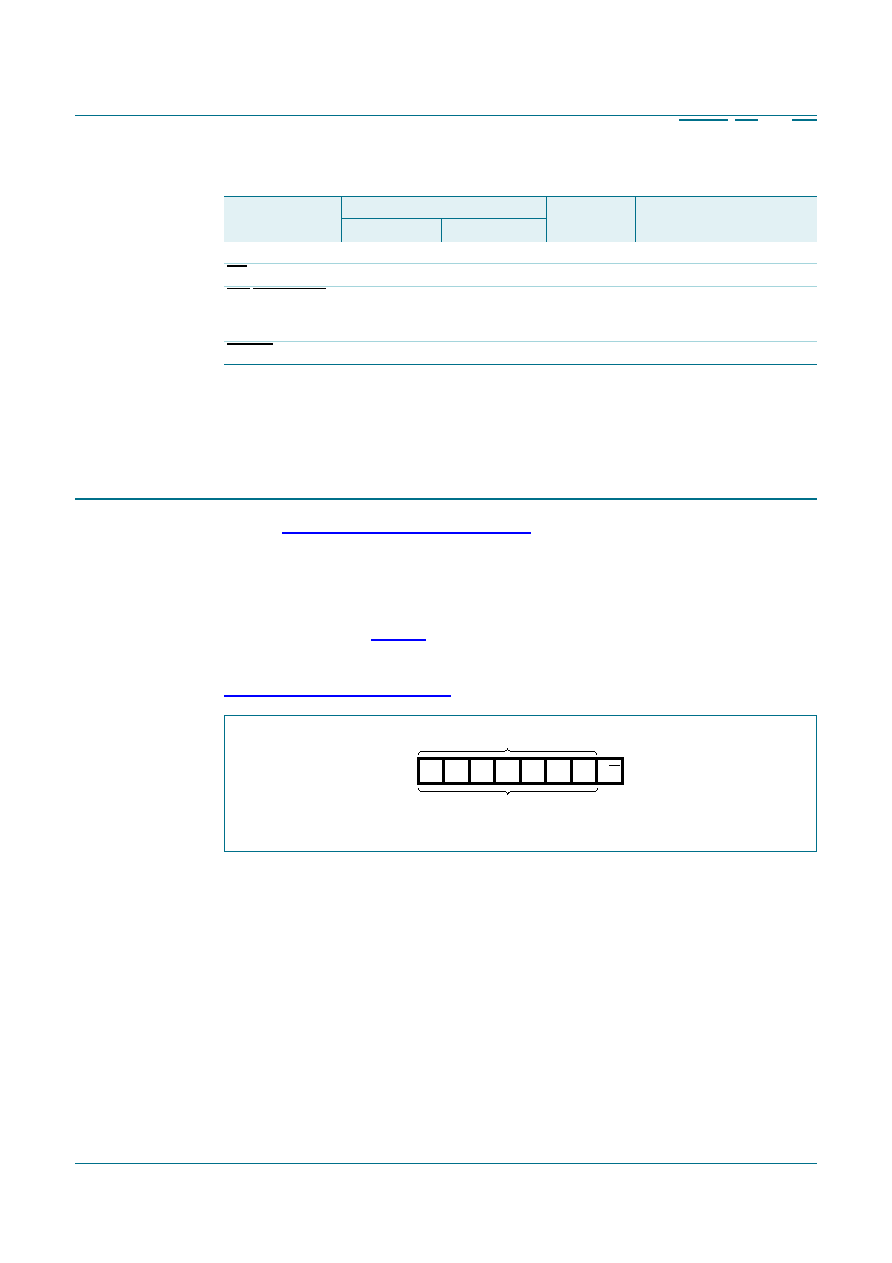
Fig 5.
PCA9698 device address
R/W
002aab937
A6
A5
A4
A3
A2
A1
A0
programmable
slave address
相关PDF资料 |
PDF描述 |
|---|---|
| PCA9555D,112 | IC I/O EXPANDER I2C 16B 24SOIC |
| PCA9555DB,112 | IC I/O EXPANDER I2C 16B 24SSOP |
| PCA9555PW,112 | IC I/O EXPANDER I2C 16B 24TSSOP |
| 5-531478-4 | CONT.MINI-LEAF STRIP |
| 5-583857-5 | TWIN LEAF DUMMY CONTACT |
相关代理商/技术参数 |
参数描述 |
|---|---|
| PCA9698DGG | 功能描述:接口-I/O扩展器 I2C I/O EXPANDER GP RoHS:否 制造商:NXP Semiconductors 逻辑系列: 输入/输出端数量: 最大工作频率:100 kHz 工作电源电压:1.65 V to 5.5 V 工作温度范围:- 40 C to + 85 C 安装风格:SMD/SMT 封装 / 箱体:HVQFN-16 封装:Reel |
| PCA9698DGG,512 | 功能描述:接口-I/O扩展器 I2C I/O EXPANDER GP RoHS:否 制造商:NXP Semiconductors 逻辑系列: 输入/输出端数量: 最大工作频率:100 kHz 工作电源电压:1.65 V to 5.5 V 工作温度范围:- 40 C to + 85 C 安装风格:SMD/SMT 封装 / 箱体:HVQFN-16 封装:Reel |
| PCA9698DGG,518 | 功能描述:接口-I/O扩展器 40BT I2C FM+TPGPIO IN-RS-PU OE RoHS:否 制造商:NXP Semiconductors 逻辑系列: 输入/输出端数量: 最大工作频率:100 kHz 工作电源电压:1.65 V to 5.5 V 工作温度范围:- 40 C to + 85 C 安装风格:SMD/SMT 封装 / 箱体:HVQFN-16 封装:Reel |
| PCA9698DGG/S911,51 | 功能描述:接口-I/O扩展器 40BT I2C FM+TPGPIO IN-RS-PU OE RoHS:否 制造商:NXP Semiconductors 逻辑系列: 输入/输出端数量: 最大工作频率:100 kHz 工作电源电压:1.65 V to 5.5 V 工作温度范围:- 40 C to + 85 C 安装风格:SMD/SMT 封装 / 箱体:HVQFN-16 封装:Reel |
| PCA9698DGG/S911-T | 功能描述:接口-I/O扩展器 40BT I2C FM+TPGPIO IN-RS-PU OE RoHS:否 制造商:NXP Semiconductors 逻辑系列: 输入/输出端数量: 最大工作频率:100 kHz 工作电源电压:1.65 V to 5.5 V 工作温度范围:- 40 C to + 85 C 安装风格:SMD/SMT 封装 / 箱体:HVQFN-16 封装:Reel |
发布紧急采购,3分钟左右您将得到回复。