- 您现在的位置:买卖IC网 > PDF目录367818 > PCF8558 (NXP Semiconductors N.V.) Universal LCD driver for small graphic panels(应用于小型图形面板的通用LCD驱动器) PDF资料下载
参数资料
| 型号: | PCF8558 |
| 厂商: | NXP Semiconductors N.V. |
| 英文描述: | Universal LCD driver for small graphic panels(应用于小型图形面板的通用LCD驱动器) |
| 中文描述: | 通用LCD驱动器小图板(应用于小型图形面板的通用液晶驱动器) |
| 文件页数: | 11/24页 |
| 文件大小: | 157K |
| 代理商: | PCF8558 |
1998 Apr 07
11
Philips Semiconductors
Objective specification
Universal LCD driver for small graphic
panels
PCF8558
CHARACTERISTICS OF THE I
2
C-BUS
The I
2
C-bus is for bidirectional, two-line communication
between different ICs or modules. The two lines are a
serial data line (SDA) and a serial clock line (SCL) which
must be connected to a positive supply via a pull-up
resistor. Data transfer may be initiated only when the bus
is not busy.
Bit transfer
One data bit is transferred during each clock pulse.
The data on the SDA line must remain stable during the
HIGH period of the clock pulse as changes in the data line
at this moment will be interpreted as control signals.
START and STOP conditions
Both data and clock lines remain HIGH when the bus is not
busy. A HIGH-to-LOW transition of the data line, while the
clock is HIGH, is defined as the START condition (S).
A LOW-to-HIGH transition of the data line while the clock
is HIGH, is defined as the STOP condition (P).
System configuration
A device transmitting a message is a 'transmitter', a device
receiving a message is the 'receiver'. The device that
controls the message flow is the 'master' and the devices
which are controlled by the master are the 'slaves'.
Acknowledge
The number of data bytes transferred between the START
and STOP conditions from transmitter to receiver is
unlimited. Each data byte of eight bits is followed by one
acknowledge bit. The acknowledge bit is a HIGH level put
on the bus by the transmitter, whereas the master
generates an extra acknowledge related clock pulse.
A slave receiver which is addressed must generate an
acknowledge after the reception of each byte. Also a
master must generate an acknowledge after the reception
of each byte that has been clocked out of the slave
transmitter. The device that acknowledges must pull down
the SDA line during the acknowledge clock pulse, so that
the SDA line is stable LOW during the HIGH period of the
acknowledge related clock pulse (set-up and hold times
must be taken into consideration). A master receiver must
signal the end of a data transmission to the transmitter by
not
generating an acknowledge on the last byte that has
been clocked out of the slave. In this event the transmitter
must leave the data line HIGH to enable the master to
generate a stop condition.
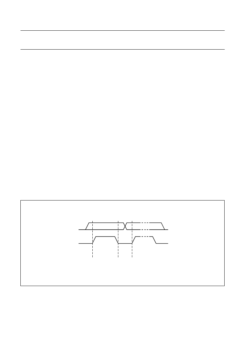
Fig.7 Bit transfer.
handbook, full pagewidth
MBC621
data line
stable;
data valid
change
of data
allowed
SDA
SCL
相关PDF资料 |
PDF描述 |
|---|---|
| PCF8558U | Universal LCD driver for small graphic panels |
| PCF8563 | Real-time clock/calendar(实时时钟/日历) |
| PCF8566 | Universal LCD driver for low multiplex rates |
| PCF8573 | Clock/calendar with Power Fail Detector |
| PCF8573P | Clock/calendar with Power Fail Detector |
相关代理商/技术参数 |
参数描述 |
|---|---|
| PCF8558U | 制造商:PHILIPS 制造商全称:NXP Semiconductors 功能描述:Universal LCD driver for small graphic panels |
| PCF8558U/10 | 制造商:PHILIPS 制造商全称:NXP Semiconductors 功能描述:Universal LCD driver for small graphic panels |
| PCF8558U/12 | 制造商:PHILIPS 制造商全称:NXP Semiconductors 功能描述:Universal LCD driver for small graphic panels |
| PCF8562 | 制造商:PHILIPS 制造商全称:NXP Semiconductors 功能描述:Universal LCD driver for low multiplex rates |
| PCF8562_09 | 制造商:PHILIPS 制造商全称:NXP Semiconductors 功能描述:Universal LCD driver for low multiplex rates |
发布紧急采购,3分钟左右您将得到回复。