- 您现在的位置:买卖IC网 > PDF目录367818 > PCF8579H (NXP SEMICONDUCTORS) LCD column driver for dot matrix graphic displays PDF资料下载
参数资料
| 型号: | PCF8579H |
| 厂商: | NXP SEMICONDUCTORS |
| 元件分类: | 显示驱动器 |
| 英文描述: | LCD column driver for dot matrix graphic displays |
| 中文描述: | LIQUID CRYSTAL DISPLAY DRIVER, PQFP64 |
| 封装: | PLASTIC, LQFP-64 |
| 文件页数: | 21/40页 |
| 文件大小: | 287K |
| 代理商: | PCF8579H |
第1页第2页第3页第4页第5页第6页第7页第8页第9页第10页第11页第12页第13页第14页第15页第16页第17页第18页第19页第20页当前第21页第22页第23页第24页第25页第26页第27页第28页第29页第30页第31页第32页第33页第34页第35页第36页第37页第38页第39页第40页
1997 Apr 01
21
Philips Semiconductors
Product specification
LCD column driver for dot matrix graphic
displays
PCF8579
9
CHARACTERISTICS OF THE I
2
C-BUS
The I
2
C-bus is for bidirectional, two-line communication
between different ICs or modules. The two lines are a
serial data line (SDA) and a serial clock line (SCL) which
must be connected to a positive supply via a pull-up
resistor. Data transfer may be initiated only when the bus
is not busy.
9.1
Bit transfer
One data bit is transferred during each clock pulse.
The data on the SDA line must remain stable during the
HIGH period of the clock pulse as changes in the data line
at this moment will be interpreted as control signals.
9.2
Start and stop conditions
Both data and clock lines remain HIGH when the bus is not
busy. A HIGH-to-LOW transition of the data line, while the
clock is HIGH, is defined as the start condition (S).
A LOW-to-HIGH transition of the data line while the clock
is HIGH, is defined as the stop condition (P).
9.3
System configuration
A device transmitting a message is a ‘transmitter’, a device
receiving a message is the ‘receiver’. The device that
controls the message flow is the ‘master’ and the devices
which are controlled by the master are the ‘slaves’.
9.4
Acknowledge
The number of data bytes transferred between the start
and stop conditions from transmitter to receiver is
unlimited. Each data byte of eight bits is followed by one
acknowledge bit. The acknowledge bit is a HIGH level put
on the bus by the transmitter, whereas the master
generates an extra acknowledge related clock pulse.
A slave receiver which is addressed must generate an
acknowledge after the reception of each byte. Also a
master must generate an acknowledge after the reception
of each byte that has been clocked out of the slave
transmitter. The device that acknowledges must pull down
the SDA line during the acknowledge clock pulse, so that
the SDA line is stable LOW during the HIGH period of the
acknowledge related clock pulse (set-up and hold times
must be taken into consideration). A master receiver must
signal the end of a data transmission to the transmitter by
not
generating an acknowledge on the last byte that has
been clocked out of the slave. In this event the transmitter
must leave the data line HIGH to enable the master to
generate a stop condition.
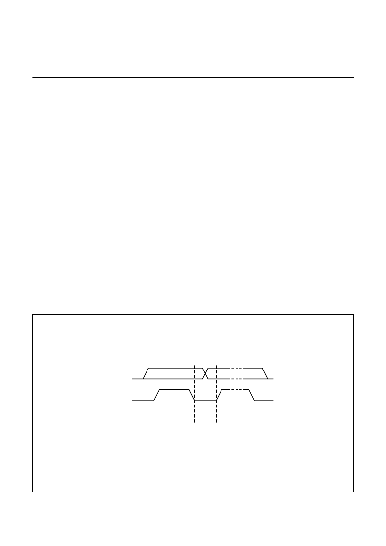
Fig.13 Bit transfer.
MBA607
data line
stable;
data valid
change
of data
allowed
SDA
SCL
相关PDF资料 |
PDF描述 |
|---|---|
| PCF8582C-2 | 256 to 1024 x 8-bit CMOS EEPROMs with I2C-bus interface |
| PCF85XXC-2 | 2 POLE 480VAC 30A AC CONTROL |
| PCF8594C-2 | 256 to 1024 x 8-bit CMOS EEPROMs with I2C-bus interface |
| PCF8594C-2P | PCF85xxC-2 family 256 to 1024 ⅴ 8-bit CMOS EEPROMs with I2C-bus interface |
| PCF8594C-2P02 | 512 X 8-bit CMOS EEPROM with I2C-bus interface |
相关代理商/技术参数 |
参数描述 |
|---|---|
| PCF8579H/1 | 功能描述:LCD 驱动器 DOT MATRIX LCD DRVR (COLUMN) RoHS:否 制造商:Maxim Integrated 数位数量:4.5 片段数量:30 最大时钟频率:19 KHz 工作电源电压:3 V to 3.6 V 最大工作温度:+ 85 C 最小工作温度:- 20 C 封装 / 箱体:PDIP-40 封装:Tube |
| PCF8579H/1,157 | 功能描述:LCD 驱动器 DOT MATRIX LCD DRVR RoHS:否 制造商:Maxim Integrated 数位数量:4.5 片段数量:30 最大时钟频率:19 KHz 工作电源电压:3 V to 3.6 V 最大工作温度:+ 85 C 最小工作温度:- 20 C 封装 / 箱体:PDIP-40 封装:Tube |
| PCF8579HT/1 | 功能描述:LED照明驱动器 LCD COLM DRVR for dot matrix GPX DISP RoHS:否 制造商:STMicroelectronics 输入电压:11.5 V to 23 V 工作频率: 最大电源电流:1.7 mA 输出电流: 最大工作温度: 安装风格:SMD/SMT 封装 / 箱体:SO-16N |
| PCF8579HT/1,518 | 制造商:NXP Semiconductors 功能描述: |
发布紧急采购,3分钟左右您将得到回复。