- 您现在的位置:买卖IC网 > PDF目录296796 > PDM31034SA15SOTY 128K X 8 STANDARD SRAM, 15 ns, PDSO32 PDF资料下载
参数资料
| 型号: | PDM31034SA15SOTY |
| 元件分类: | SRAM |
| 英文描述: | 128K X 8 STANDARD SRAM, 15 ns, PDSO32 |
| 文件页数: | 2/8页 |
| 文件大小: | 309K |
| 代理商: | PDM31034SA15SOTY |
PRELIMINARY
PDM31034
2
Rev. 1.4 - 4/17/98
Absolute Maximum Ratings (1)
NOTE: 1. Stresses greater than those listed under ABSOLUTE MAXIMUM RATINGS may
cause permanent damage to the device. This is a stress rating only and functional
operation of the device at these or any other conditions above those indicated in the
operational sections of this specication is not implied. Exposure to absolute maxi-
mum rating conditions for extended periods may affect reliability.
2. Appropriate thermal calculations should be performed in all cases and specically for
those where the chosen package has a large thermal resistance (e.g., TSOP). The cal-
culation should be of the form: Tj = Ta + P * θja where Ta is the ambient temperature, P
is average operating power and
θ
ja the thermal resistance of the package. For this
product, use the following
θ
ja values:
SOJ: 72o C/W
TSOP: 95o C/W
Symbol
Rating
Com’l.
Ind.
Auto.
Unit
VTERM
Terminal Voltage with Respect to VSS
–0.5 to +4.6
V
TBIAS
Temperature Under Bias
–55 to +125
–65 to +135
–65 to +145
°C
TSTG
Storage Temperature
–55 to +125
–65 to +150
°C
PT
Power Dissipation
900
mW
IOUT
DC Output Current
50
mA
Tj
Maximum Junction Temperature (2)
125
145
°C
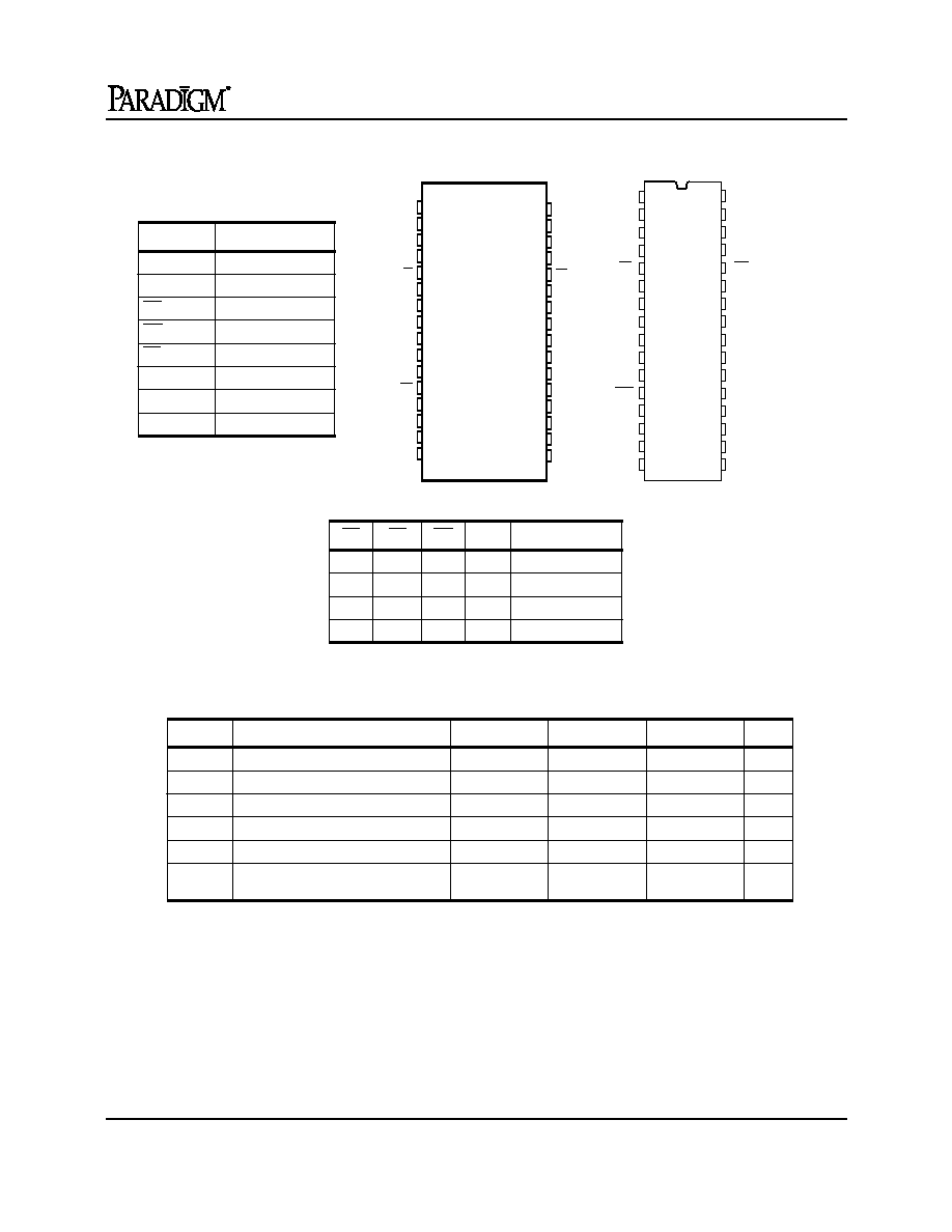
A3
A2
A1
A0
CE
I/O0
I/O1
Vcc
Vss
I/O2
I/O3
WE
A16
A15
A14
A13
32
31
30
29
28
27
26
25
24
23
22
21
20
19
18
17
A4
A5
A6
A7
OE
I/O7
I/O6
Vss
Vcc
I/O5
I/O4
A8
A9
A10
A11
A12
1
2
3
4
5
6
7
8
9
10
11
12
13
14
15
16
1
2
3
4
5
6
7
8
9
10
11
12
15
16
17
18
19
20
21
22
23
24
A3
A2
A1
A0
CE
I/O0
I/O1
Vcc
Vss
I/O2
I/O3
WE
A16
A15
A14
A13
A4
A5
A6
A7
OE
I/O7
I/O6
Vss
Vcc
I/O5
I/O4
A8
A9
A10
A11
A12
13
14
25
26
27
28
29
30
31
32
Truth Table(1)
NOTE: 1. H = VIH, L = VIL, X = DON’T CARE
CE
OE
WE
I/O
MODE
LL
H
DOUT
Read
LX
L
DIN
Write
L
H
Hi-Z
Output Disable
H
X
Hi-Z
Standby
Pin Description
Name
Description
A16-A0
Address Inputs
I/O7-I/O0
Data Inputs/Outputs
OE
Output Enable Input
WE
Write Enable Input
CE
Chip Enable Input
NC
No Connect
VCC
Power (+3.3V)
VSS
Ground
Pin Conguration
SOJ
TSOP (II)
相关PDF资料 |
PDF描述 |
|---|---|
| PDM31038SA12T | 256K X 4 STANDARD SRAM, 12 ns, PDSO32 |
| PDM31096SA25SOTY | 512K X 8 STANDARD SRAM, 25 ns, PDSO36 |
| PDM31256L25T | 32K X 8 STANDARD SRAM, 25 ns, PDSO28 |
| PDM31356S12SOTY | 32K X 8 STANDARD SRAM, 12 ns, PDSO32 |
| PDM31564SA12T | 256K X 16 STANDARD SRAM, 12 ns, PDSO44 |
相关代理商/技术参数 |
参数描述 |
|---|---|
| PDM31096 | 制造商:未知厂家 制造商全称:未知厂家 功能描述:4 Megabit 3.3V Static RAM 512K x 8-Bit |
| PDM31096SA10SO | 制造商:未知厂家 制造商全称:未知厂家 功能描述:4 Megabit 3.3V Static RAM 512K x 8-Bit |
| PDM31096SA10SOA | 制造商:未知厂家 制造商全称:未知厂家 功能描述:4 Megabit 3.3V Static RAM 512K x 8-Bit |
| PDM31096SA10SOATR | 制造商:未知厂家 制造商全称:未知厂家 功能描述:4 Megabit 3.3V Static RAM 512K x 8-Bit |
| PDM31096SA10SOATY | 制造商:未知厂家 制造商全称:未知厂家 功能描述:4 Megabit 3.3V Static RAM 512K x 8-Bit |
发布紧急采购,3分钟左右您将得到回复。