- 您现在的位置:买卖IC网 > PDF目录69043 > PE3336-53 (PEREGRINE SEMICONDUCTOR CORP) PHASE LOCKED LOOP, 3000 MHz, PQCC44 PDF资料下载
参数资料
| 型号: | PE3336-53 |
| 厂商: | PEREGRINE SEMICONDUCTOR CORP |
| 元件分类: | PLL合成/DDS/VCOs |
| 英文描述: | PHASE LOCKED LOOP, 3000 MHz, PQCC44 |
| 封装: | GREEN, PLASTIC, LCC-44 |
| 文件页数: | 11/16页 |
| 文件大小: | 359K |
| 代理商: | PE3336-53 |
Product Specification
PE3336
Page 4 of 16
2005-2010 Peregrine Semiconductor Corp. All rights reserved.
Document No. 70-0033-04
│ UltraCMOS RFIC Solutions
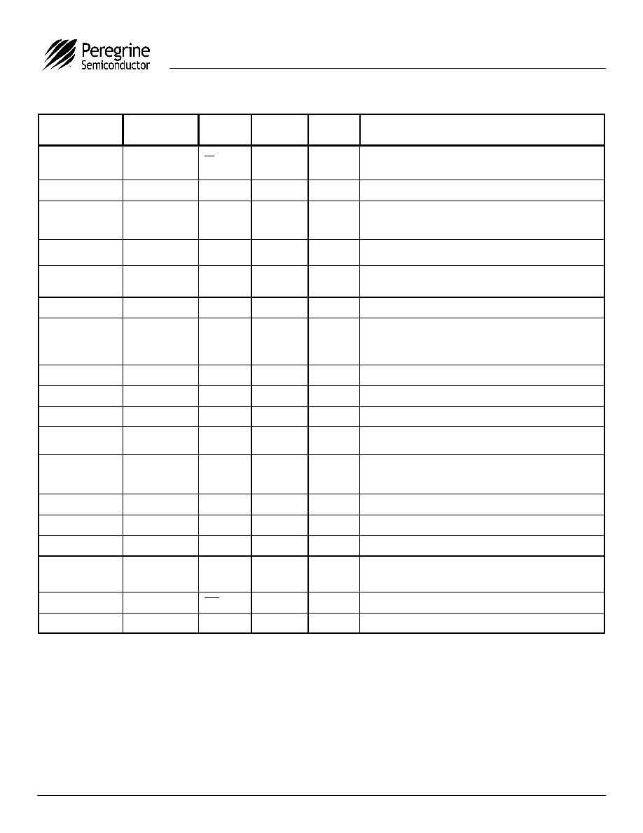
28
23
Fin
ALL
Input
Prescaler complementary input. A bypass capacitor should be
placed as close as possible to this pin and be connected in
series with a 50
resistor directly to the ground plane.
29
24
GND
ALL
Ground.
30
25
fp
ALL
Output
Monitor pin for main divider output. Switching activity can be
disabled through enhancement register programming or by
floating or grounding VDD pin 31.
31
26
VDD-fp
ALL
(Note 1)
VDD for fp. Can be left floating or connected to GND to disable
the fp output.
32
27
Dout
Serial,
Parallel
Output
Data Out. The MSEL signal and the raw prescaler output are
available on Dout through enhancement register
programming.
33
28
VDD
ALL
(Note 1)
Same as pin 1.
34
29
Cext
ALL
Output
Logical “NAND” of PD_U and PD_D terminated through an on
chip, 2 k
series resistor. Connecting Cext to an external
capacitor will low pass filter the input to the inverting amplifier
used for driving LD.
35
30
VDD
ALL
(Note 1)
Same as pin 1.
36
32
PD_D
ALL
Output
PD_D is pulse down when fp leads fc.
37
33
PD_U
ALL
PD_U is pulse down when fc leads fp.
38
35
VDD-fc
ALL
(Note 1)
VDD for fc can be left floating or connected to GND to disable
the fc output.
39
36
fc
ALL
Output
Monitor pin for reference divider output. Switching activity can
be disabled through enhancement register programming or by
floating or grounding VDD pin 38.
40
31,37
GND
ALL
Ground.
41
38,39
GND
ALL
Ground.
42
40
fr
ALL
Input
Reference frequency input.
43
41
LD
ALL
Output
Lock detect and open drain logical inversion of CEXT. When
the loop is in lock, LD is high impedance, otherwise LD is a
logic low (“0”).
44
42
Enh
Serial,
Parallel
Input
Enhancement mode. When asserted low (“0”), enhancement
register bits are functional.
N/A
34
NC
ALL
No connection.
Pin No.
(44-lead PLCC)
Pin No.
(48-lead QFN)
Pin
Name
Interface
Mode
Type
Description
Table 1. Pin Descriptions (continued)
Note 1:
All VDD pins are connected by diodes and must be supplied with the same positive voltage level.
VDD-fp and VDD-fp are used to power the fp and fc outputs and can alternatively be left floating or connected to GND to disable the fp and fc
outputs.
Note 2:
All digital input pins have 70 k
pull-down resistors to ground.
相关PDF资料 |
PDF描述 |
|---|---|
| PE3336-21 | PHASE LOCKED LOOP, 3000 MHz, PQCC44 |
| PE3336-00 | PHASE LOCKED LOOP, 3000 MHz, QCC44 |
| PE3336-22 | PHASE LOCKED LOOP, 3000 MHz, PQCC44 |
| PE3339-12 | PHASE LOCKED LOOP, PDSO20 |
| PE3339-11 | PHASE LOCKED LOOP, PDSO20 |
相关代理商/技术参数 |
参数描述 |
|---|---|
| PE3336EK | 制造商:PEREGRINE 制造商全称:PEREGRINE 功能描述:3000 MHz UltraCMOS⑩ Integer-N PLL for Low Phase Noise Applications |
| PE33370LF | 制造商:PASTERNACK 制造商全称:Pasternack Enterprises, Inc. 功能描述:CABLE ASSEMBLY RG217/U HN MALE TO HN MALE(LEAD FREE) |
| PE33383 | 制造商:PASTERNACK 制造商全称:Pasternack Enterprises, Inc. 功能描述:CABLE ASSEMBLY RG316/U BNC MALE TO TNC MALE |
| PE3339 | 制造商:PEREGRINE 制造商全称:PEREGRINE 功能描述:3.0 GHz Integer-N PLL for Low Phase Noise Applications |
| PE33399 | 制造商:PASTERNACK 制造商全称:Pasternack Enterprises, Inc. 功能描述:CABLE ASSEMBLY RG11A/U 75 OHM BNC MALE TO 75 OHM BNC MALE |
发布紧急采购,3分钟左右您将得到回复。