- 您现在的位置:买卖IC网 > PDF目录367929 > PGA2310 Stereo Audio Volume Control PDF资料下载
参数资料
| 型号: | PGA2310 |
| 英文描述: | Stereo Audio Volume Control |
| 中文描述: | 立体声音频音量控制 |
| 文件页数: | 7/16页 |
| 文件大小: | 322K |
| 代理商: | PGA2310 |
"#$%&
SBOS207B OCTOBER 2001 REVISED JUNE 2004
ANALOG INPUTS AND
OUTPUTS
The PGA2310 includes two independent channels,
referred to as the left and right channels. Each channel has
a corresponding input and output pin. The input and output
pins are unbalanced, or referenced to analog ground
(either AGNDR or AGNDL). The inputs are named V
IN
R
(pin 9) and V
IN
L (pin 16), while the outputs are named
V
OUT
R (pin 11) and V
OUT
L (pin 14).
www.ti.com
7
GENERAL DESCRIPTION
The PGA2310 is a stereo audio volume control. It may be
used in a wide array of professional and consumer audio
equipment. The PGA2310 is fabricated in a mixed-signal
BiCMOS process, as to take advantage of the superior
analog characteristics for which it offers.
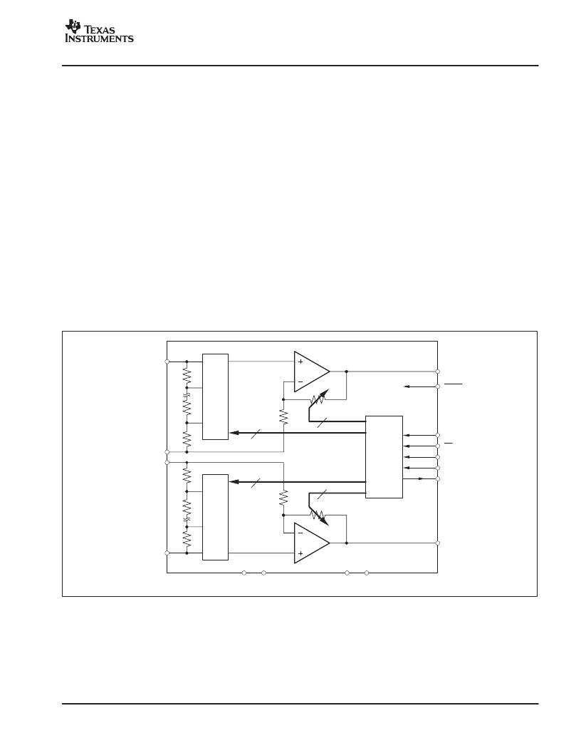
The heart of the PGA2310 is a resistor network, an analog
switch array, and a high-performance bipolar op amp
stage. The switches are used to select taps in the resistor
network that, in turn, determine the gain of the amplifier
stage. Switch selections are programmed using a serial
control port. The serial port allows connection to a wide
variety of host controllers. Figure 1 shows a functional
block diagram of the PGA2310.
POWER-UP STATE
On power up, all internal flip-flops are reset. The gain byte
value for both the left and right channels are set to 00
HEX
,
or mute condition. The gain will remain at this setting until
the host controller programs new settings for each channel
via the serial control port.
The input and output pins may swing within 1.5V of the
analog power supplies, V
A
+ (pin 12) and V
A
(pin 13).
Given V
A
+ = +15V and V
A
= 15V, the maximum input or
output voltage range is 27V
PP
.
It is important to drive the PGA2310 with a low source
impedance. If a source impedance of greater than 600
is
used, the distortion performance of the PGA2310 will
begin to degrade.
MUX
Serial
Control
Port
MUX
ZCEN
CS
SCLK
SDI
SDO
MUTE
V
OUT
R
V
OUT
L
V
IN
L
AGNDL
AGNDR
V
IN
R
V
A
+V
A
V
D
+ DGND
12
13
4
5
11
7
3
6
2
1
8
14
16
15
10
9
8
8
8
8
Figure 1. PGA2310 Block Diagram
相关PDF资料 |
PDF描述 |
|---|---|
| PGA2310PA | Stereo Audio Volume Control |
| PGA2310UA | Stereo Audio Volume Control |
| PGA2311PAG4 | Stereo Audio VOLUME CONTROL |
| PGA2311PG4 | Stereo Audio VOLUME CONTROL |
| PGA2311UAG4 | Stereo Audio VOLUME CONTROL |
相关代理商/技术参数 |
参数描述 |
|---|---|
| PGA2310_06 | 制造商:BB 制造商全称:BB 功能描述:Stereo Audio Volume Control |
| PGA2310_08 | 制造商:BB 制造商全称:BB 功能描述:Stereo Audio Volume Control |
| PGA2310EVM | 功能描述:音频 IC 开发工具 PGA2310 Eval Mod RoHS:否 制造商:Texas Instruments 产品:Evaluation Kits 类型:Audio Amplifiers 工具用于评估:TAS5614L 工作电源电压:12 V to 38 V |
| PGA2310PA | 功能描述:音频放大器 AUDIO VOLUME CONTROL RoHS:否 制造商:STMicroelectronics 产品:General Purpose Audio Amplifiers 输出类型:Digital 输出功率: THD + 噪声: 工作电源电压:3.3 V 电源电流: 最大功率耗散: 最大工作温度: 安装风格:SMD/SMT 封装 / 箱体:TQFP-64 封装:Reel |
| PGA2310PA | 制造商:Texas Instruments 功能描述:AUDIO VOLUME CONTROL 2310 PDIP16 |
发布紧急采购,3分钟左右您将得到回复。