- 您现在的位置:买卖IC网 > PDF目录97633 > PI3A4627TX (PERICOM SEMICONDUCTOR CORP) 1-CHANNEL, SGL POLE SGL THROW SWITCH, PDSO5 PDF资料下载
参数资料
| 型号: | PI3A4627TX |
| 厂商: | PERICOM SEMICONDUCTOR CORP |
| 元件分类: | 多路复用及模拟开关 |
| 英文描述: | 1-CHANNEL, SGL POLE SGL THROW SWITCH, PDSO5 |
| 封装: | SOT-23, 5 PIN |
| 文件页数: | 2/8页 |
| 文件大小: | 502K |
| 代理商: | PI3A4627TX |
PI3A4627
3.0V, SOTiny Single-Supply
0.4 SPST (NC) CMOS Analog Switch
2
PS8715A
07/07/04
Caution: Stresses beyond those listed under “Absolute Maximum Ratings” may cause permanent damage to the device. This is a
stress only rating and operation of the device at these or any other conditions beyond those indicated in the operational sections of
this specification is not implied.
Absolute Maximum Ratings
Voltages Referenced to GND
VCC.......................................................................–0.5V to +3.6V
VIN, VCOM, VNC, VNO (1)............................ –0.5V to VCC +0.3V
or 30mA, whichever occurs first
Current (any terminal).....................................................±200mA
Peak Current, COM, NO, NC
(Pulsed at 1ms, 10% duty cycle).....................................±400mA
Note:
1. Signals on NC, NO, COM, or IN exceeding VCC or GND are clamped by internal diodes. Limit forward diode current to 30mA.
Thermal Information
Continuous Power Dissipation
SOT-23 (derate 7.1mW/C above +70C)........................... 0.5W
Storage Temperature ........................................–65C to +150C
Lead Temperature (soldering, 10s) ................................. +300C
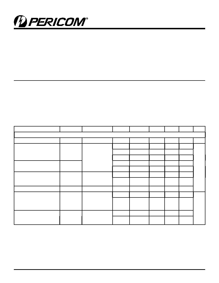
Electrical Specifications - Single +3.3V Supply
(VCC = +3.3V ± 10%, GND = 0V, VIH = 1.4V, VIL = 0.5V)
Description
Parameters
Test Conditions
Package Temp.(°C) Min.(1) Typ.(2) Max.(1) Units
Analog Switch
Analog Signal Range(3)
VANALOG
Full
0
VCC
V
On Resistance
RON
VCC = 2.7V,
ICOM = 100mA,
VNO or VNC =
1.5V
25
0.4
SOT23
0.5
TDFN
Full
0.6
On-Resistance Match Be-
tween Channels(4)
RON
25
0.05
Full
0.06
On-Resistance
Flatness(5)
RFLAT(ON)
VCC =2.7V, ICOM
= 100mA, VNO or
VNC = 0.8V, 2.0V
25
0.1
Full
0.1
NO or NC Off Leakage Cur-
rent(6)
ICOM(OFF) or
INC(OFF)
VCC =3.3V, VCOM
= 0V,
VNO or VNC =
+2.0V
25
–1
1
nA
Full
–20
10
COM On Leakage Current(6) ICOM(ON)
VCC =3.3V, VCOM
= +2.0V VNO or
VNC = +2.0V
25
–2
2
Full
–20
20
相关PDF资料 |
PDF描述 |
|---|---|
| PI5A100S | QUAD 2-CHANNEL, SGL POLE DOUBLE THROW SWITCH, PDSO16 |
| PI5A126UEX | DUAL 1-CHANNEL, SGL POLE SGL THROW SWITCH, PDSO8 |
| PI5A126WE | DUAL 1-CHANNEL, SGL POLE SGL THROW SWITCH, PDSO8 |
| PI5A126W | DUAL 1-CHANNEL, SGL POLE SGL THROW SWITCH, PDSO8 |
| PI5A4597ACX | 1-CHANNEL, SGL POLE SGL THROW SWITCH, PDSO5 |
相关代理商/技术参数 |
参数描述 |
|---|---|
| PI3A4628 | 制造商:未知厂家 制造商全称:未知厂家 功能描述:Analog | 3.0V. SOTiny. 0.4-Ohm SPST Analog Switch |
| PI3A4629 | 制造商:未知厂家 制造商全称:未知厂家 功能描述:Analog | 3.0V. SOTiny. 0.4-Ohm SPST Analog Switch |
| PI3B16209 | 制造商:PERICOM 制造商全称:Pericom Semiconductor Corporation 功能描述:3.3V, 18-Bit Bus Exchange Switch |
| PI3B16209A | 制造商:未知厂家 制造商全称:未知厂家 功能描述:Bus Exchanger |
| PI3B16209A48 | 制造商:未知厂家 制造商全称:未知厂家 功能描述:Bus Exchanger |
发布紧急采购,3分钟左右您将得到回复。