- 您现在的位置:买卖IC网 > PDF目录65870 > PI3V514-ABE (PERICOM SEMICONDUCTOR CORP) 4-CHANNEL, VIDEO MULTIPLEXER, PDSO48 PDF资料下载
参数资料
| 型号: | PI3V514-ABE |
| 厂商: | PERICOM SEMICONDUCTOR CORP |
| 元件分类: | 多路复用及模拟开关 |
| 英文描述: | 4-CHANNEL, VIDEO MULTIPLEXER, PDSO48 |
| 封装: | 0.150 INCH, GREEN, BQSOP-48 |
| 文件页数: | 3/9页 |
| 文件大小: | 367K |
| 代理商: | PI3V514-ABE |
3
PS8893A
05/29/07
PI3V514-A
Low On-Resistance, 3.3V High-Bandwidth 5-port,
4:1 Mux/DeMux Video Switch w/ Enhanced ESD Support
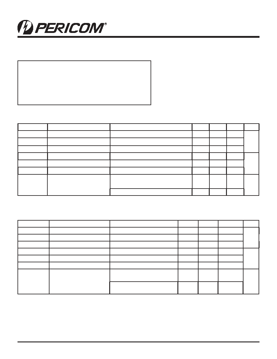
Storage Temperature ................................................ –65°C to +150°C
Ambient Temperature with Power Applied ............... –40°C to +85°C
Supply Voltage to Ground Potential ........................... –0.5V to +4.6V
DC Input Voltage ........................................................ –0.5V to +6.0V
DC Output Current................................................................... 120mA
Power Dissipation ........................................................................0.5W
Note:
Stresses greater than those listed under MAXIMUM
RATINGS may cause permanent damage to the device. This is a
stress rating only and functional operation of the device at these
or any other conditions above those indicated in the operational
sections of this specication is not implied. Exposure to absolute
maximum rating conditions for extended periods may affect re-
liability.
Maximum Ratings
(Above which the useful life may be impaired. For user guidelines, not tested.)
DC Electrical Characteristics, 3.3V Supply (Over the Operating Range, TA = –40°C to +85°C, VCC = 3.3V ±10%)
Parameters
Description
Test Conditions(1)
Min.
Typ(2)
Max.
Units
VIH
Input HIGH Voltage
Guaranteed Logic HIGH Level
2.0
V
VIL
Input LOW Voltage
Guaranteed Logic LOW Level
–0.5
0.8
VIK
Clamp Diode Voltage
VCC = Min., IIN = –18 mA
-1.3
–1.8
IIH
Input HIGH Current
VCC = Max., VIN = VCC
±1
μA
IIL
Input LOW Current
VCC = Max., VIN = GND
±1
IOZH
High Impedance Output Current 0 ≤ Y, In ≤ VCC
±1
RON
Switch On-Resistance(3)
VCC = Min., VIN = 0V,
ION = 48 mA or -64mA
46
Ω
VCC = Min., VIN = 3.6V, ION = -15 mA
5
8
DC Electrical Characteristics, 2.5V Supply (Over Operating Range, TA = –40°C to +85°C, VCC = 2.5V ± 10%)
Parameters(4)
Description
Test Conditions (1)
Min.
Typ. (2)
Max.
Units
VIH
Input HIGH Voltage
Guaranteed Logic HIGH Level
1.8
–
VCC + 0.3
V
VIL
Inout LOW Voltage
Guaranteed Logic LOW Level
–0.3
–
0.8
VIK
Clamp Diode Voltage
VCC = Max., IIN = –6mA
–
–0.7
–1.8
IIH
Input HIGH Current
VCC = Max., VIN = VCC
––
±1
μA
IIL
Input LOW Current
VCC = Max., VIN = GND
–
±1
IOZH
High Impedance Current
0 ≤ Y, In ≤ VCC
––
±1
RON
Switch On-Resistance(3)
VCC = Min., VIN = 0V,
ION = –48mA
–6
8
Ω
VCC = Min., VIN = 2.25V,
ION = -15mA
–7
14
Notes:
1.
For Max. or Min. conditions, use appropriate value specied under Electrical Characteristics for the applicable device type.
2.
Typical values are at VCC = 2.5V, TA = 25°C ambient and maximum loading.
3.
Measured by the voltage drop between Y and In pin at indicated current through the switch. On-Resistance is determined
by the lower of the voltages on the two (Y, In) pins.
4.
This parameter is determined by device characterization but is not production tested.
DRAFT
VERSION
相关PDF资料 |
PDF描述 |
|---|---|
| PI3V514-ABEX | 4-CHANNEL, VIDEO MULTIPLEXER, PDSO48 |
| PI4S706RW | 1-CHANNEL POWER SUPPLY MANAGEMENT CKT, PDSO8 |
| PI4S707W | 1-CHANNEL POWER SUPPLY MANAGEMENT CKT, PDSO8 |
| PI4S708SW | 1-CHANNEL POWER SUPPLY MANAGEMENT CKT, PDSO8 |
| PI4S708TWE | 1-CHANNEL POWER SUPPLY MANAGEMENT CKT, PDSO8 |
相关代理商/技术参数 |
参数描述 |
|---|---|
| PI3V514B | 制造商:PERICOM 制造商全称:Pericom Semiconductor Corporation 功能描述:LOW ON RESISTANCE 3.3V HIGH BANDWIDTH 5-PORT 4:1 MUX/DEMUX VIDEOSWITCH |
| PI3V514BE | 功能描述:多路器开关 IC 5-Channel 3.3V 4:1 Video Switch RoHS:否 制造商:Texas Instruments 通道数量:1 开关数量:4 开启电阻(最大值):7 Ohms 开启时间(最大值): 关闭时间(最大值): 传播延迟时间:0.25 ns 工作电源电压:2.3 V to 3.6 V 工作电源电流: 最大工作温度:+ 85 C 安装风格:SMD/SMT 封装 / 箱体:UQFN-16 |
| PI3V514BEX | 功能描述:多路器开关 IC Low On Resistance 3.3V High RoHS:否 制造商:Texas Instruments 通道数量:1 开关数量:4 开启电阻(最大值):7 Ohms 开启时间(最大值): 关闭时间(最大值): 传播延迟时间:0.25 ns 工作电源电压:2.3 V to 3.6 V 工作电源电流: 最大工作温度:+ 85 C 安装风格:SMD/SMT 封装 / 箱体:UQFN-16 |
| PI3V520ZFE | 制造商:Pericom Semiconductor Corporation 功能描述: |
| PI3V712-AZHE | 功能描述:多路器开关 IC 7 Channel VGA Switch RoHS:否 制造商:Texas Instruments 通道数量:1 开关数量:4 开启电阻(最大值):7 Ohms 开启时间(最大值): 关闭时间(最大值): 传播延迟时间:0.25 ns 工作电源电压:2.3 V to 3.6 V 工作电源电流: 最大工作温度:+ 85 C 安装风格:SMD/SMT 封装 / 箱体:UQFN-16 |
发布紧急采购,3分钟左右您将得到回复。