参数资料
| 型号: | PI4ULS3V08ZFEX |
| 厂商: | Pericom |
| 文件页数: | 2/7页 |
| 文件大小: | 0K |
| 描述: | IC VOLT TRANSLATOR 8BIT 36TQFN |
| 标准包装: | 3,500 |
| 系列: | ULS |
| 逻辑功能: | 电平移位器,双向,3 态 |
| 位数: | 8 |
| 输入类型: | 电压 |
| 输出类型: | 电压 |
| 数据速率: | 180Mbps |
| 通道数: | 8 |
| 输出/通道数目: | 1 |
| 差分 - 输入:输出: | 无/无 |
| 传输延迟(最大): | 4ns |
| 电源电压: | 1.2 V ~ 3.6 V |
| 工作温度: | -40°C ~ 85°C |
| 封装/外壳: | 36-WFQFN 裸露焊盘 |
| 供应商设备封装: | 36-TQFN-EP(6x5) |
| 包装: | 带卷 (TR) |
|||||||||||||||||||||||||||||||||||||||||||||||||||||||||||||||||||||||||||||||||||||||||||||||||||||||||||||||||||||||||||||||||||||||||||||||||||||||||||||||||||||||||||||||||||||||||||||||||||||||||||||||||||||||||||||||||||||||||||||||||||||||||||||||||||||||||||||||||||||||||||||||||||||||||||||||||||||||||||||||||||||||
2013-07-0006
PT0487
07/12/13
2
PI4ULS3V08
1.2V to 3.6V Universal Bidirectional Level
Shifter with Automatic Direction Control
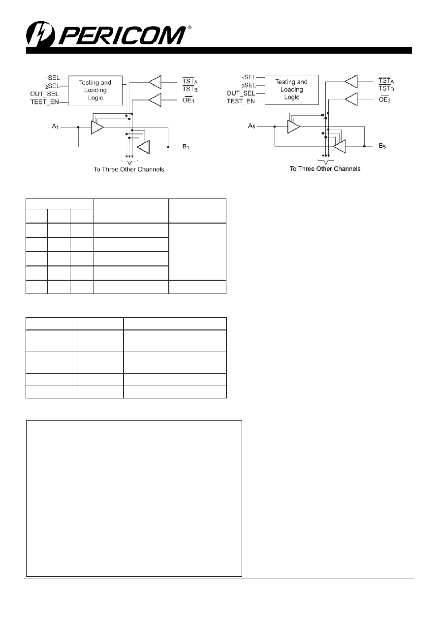
Block Diagram
Figure 1. Block Diagram
Truth Table
Test Mode / Output Impedance Select
Maximum Ratings
StorageTemperature...................................................................................-65oC to +150oC
DC Supply Voltage VCCA............................................................................-0.5V to +4.6V
DC Supply Voltage VCCB............................................................................-0.5V to +4.6V
Enable Control Pin DC Input Voltage
....................................................-0.5Vto+4.6V
Voltage Range applied to any I/O pins in the high-impedance
or Power-Off state VIOZ(A)
.................................................................-0.5Vto+4.6V
Voltage Range applied to any I/O pins in the high-impedance
or Power-Off state VIOZ(B)
.................................................................-0.5Vto+4.6V
Voltage Range applied to any I/O pins in the high or Low
state VIO(A)
................................................................................. -0.5Vto VCCA+0.5V
Voltage Range applied to any I/O pins in the high or Low
state VIO(B)
..................................................................................-0.5Vto VCCB+0.5V
Input clamp Current (VI < 0)
..............................................................................-50mA
Ourput clamp current (VO < 0)
..........................................................................-50mA
Continuous output current
.................................................................................±20mA
Continuous current through VCCA, VCCB or GNDPin
..............................±100mA
Inputs
(1)
Outputs Loading(2)
Operation
xOE 2SEL 1SEL
L
CL ≤ 50pF
Bus B data to Bus
A, or Bus A data
to Bus B
L
H
CL ≤ 30pF
L
H
L
CL ≤ 20pF
L
H
CL ≤ 10pF
H
X
-
Z (Isolation)
TEST_EN
Out_SEL
Condition
L
Normal Operation
Low output impedance 300Ω
L
H
Normal Operation
High output impedance 2.2KΩ
H
L
Test_MODE A → B
H
Test_MODE B → A
Note:
1
The input negative voltage and output voltage
ratings may be exceeded if the input and output
current ratings are observed.
2
This value is limited to 3.6V maximum.
3
Stresses
greater
than
those
listed
under
MAXIMUM RATINGS may cause permanent
damage to the device. This is a stress rating only
and functional operation of the device at these or
any other condi-tions above those indicated in the
operational sec-tions of this specification is not
implied. Exposure to absolute maximum rating
conditions
for
extended
periods
may
affect
reliability.
Note:
1. H = HIGH Signal Level,
L = LOW Signal Level
X = Don’t Care or Irrelevant,
Z = High Impedance
2. Refer to Figure 2 for output Loading Chart
相关PDF资料 |
PDF描述 |
|---|---|
| PI4ULS3V16AE | IC VOLT TRANSLATOR 56-TSSOP |
| PI4ULS5V102UEX | IC LOGIC TRANSLATOR |
| PI4ULS5V104GAEX | IC LOGIC TRANSLATOR |
| PI5C16210VE | IC 20-BIT BUS SW 2PORT 48-SSOP |
| PI5C16211A | IC 24-BIT BUS SWITCH 56-TSSOP |
相关代理商/技术参数 |
参数描述 |
|---|---|
| PI4ULS3V16 | 制造商:PERICOM 制造商全称:Pericom Semiconductor Corporation 功能描述:1.2V to 3.6V Universal Bi-directional Level Shifter with Automatic Direction Control |
| PI4ULS3V16_07 | 制造商:PERICOM 制造商全称:Pericom Semiconductor Corporation 功能描述:1.2V to 3.6V Universal Bi-directional Level Shifter with Automatic Direction Control |
| PI4ULS3V16A | 制造商:PERICOM 制造商全称:Pericom Semiconductor Corporation 功能描述:1.2V to 3.6V Universal Bi-directional Level Shifter with Automatic Direction Control |
| PI4ULS3V16AE | 功能描述:转换 - 电压电平 16bit Auto Direction Sensing Volt Trans RoHS:否 制造商:Micrel 类型:CML/LVDS/LVPECL to LVCMOS/LVTTL 传播延迟时间:1.9 ns 电源电流:14 mA 电源电压-最大:3.6 V 电源电压-最小:3 V 最大工作温度:+ 85 C 安装风格:SMD/SMT 封装 / 箱体:MLF-8 |
| PI4ULS3V16AEX | 功能描述:转换 - 电压电平 Universal Bidirectional Level RoHS:否 制造商:Micrel 类型:CML/LVDS/LVPECL to LVCMOS/LVTTL 传播延迟时间:1.9 ns 电源电流:14 mA 电源电压-最大:3.6 V 电源电压-最小:3 V 最大工作温度:+ 85 C 安装风格:SMD/SMT 封装 / 箱体:MLF-8 |
发布紧急采购,3分钟左右您将得到回复。