- 您现在的位置:买卖IC网 > PDF目录365356 > PI5C162244B (Pericom Semiconductor Corp.) Micropower, Regulated 5V Charge Pump DC/DC Converter; Package: SO; No of Pins: 8; Temperature Range: -40°C to +85°C PDF资料下载
参数资料
| 型号: | PI5C162244B |
| 厂商: | Pericom Semiconductor Corp. |
| 英文描述: | Micropower, Regulated 5V Charge Pump DC/DC Converter; Package: SO; No of Pins: 8; Temperature Range: -40°C to +85°C |
| 中文描述: | 总线开关 |
| 文件页数: | 3/3页 |
| 文件大小: | 38K |
| 代理商: | PI5C162244B |
PI5C16244/162244
16-BIT BUS SWITCH BUFFER
124
PS7024B 09/17/96
12345678901234567890123456789012123456789012345678901234567890121234567890123456789012345678901212345678901234567890123456789012123456789012
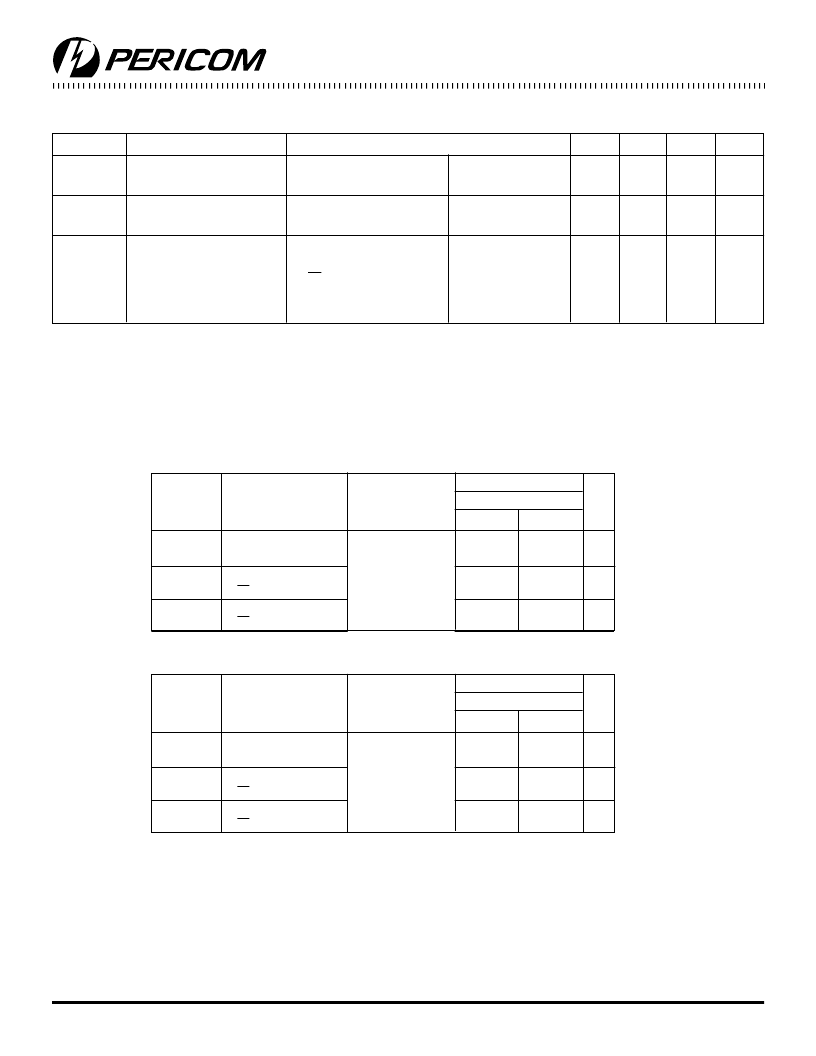
Power Supply Characteristics
Parameters Description
Test Conditions
(1)
Min.
Typ
(2)
Max.
Units
I
CC
Quiescent Power
Supply Current
V
CC
= Max.
V
IN
= GND or V
CC
—
0.1
3.0
μA
I
CC
Supply Current per
Input @ TTL HIGH
V
CC
= Max.
V
IN
= 3.4V
(3)
—
—
2.5
mA
I
CCD
Supply Current per
Input per MHz
(4)
V
CC
= Max.,
A and B Pins Open
nBE = GND
Control Input Toggling
50% Duty Cycle
—
—
0.25
mA/
MHz
Notes:
1. For Max. or Min. conditions, use appropriate value specified under Electrical Characteristics for the applicable device.
2. Typical values are at Vcc = 5.0V, +25°C ambient.
3. Per TTL driven input (V
IN
= 3.4V, control inputs only); A and B pins do not contribute to Icc.
4. This current applies to the control inputs only and represent the current required to switch internal capacitance at the specified
frequency. The A and B inputs generate no significant AC or DC currents as they transition. This parameter is not tested, but is
guaranteed by design.
PI5C16244 Switching Characteristics over Operating Range
PI5C16244
Com.
Parameters
Description
Conditions
(1)
Min
Max
Unit
t
PLH
t
PHL
t
PZH
t
PZL
t
PHZ
t
PLZ
Propagation Delay
(2,3)
xAx to xBx
Bus Enable Time
X
BE to xAx or xBx
Bus Disable Time
X
BE to xAx or xBx
C
L
= 50 pF
R
L
= 500
—
0.25
ns
1.5
5.6
ns
1.5
5.2
ns
Notes:
1. See test circuit and wave forms.
2. This parameter is guaranteed but not tested on Propagation Delays.
3. The bus switch contributes no propagational delay other than the RC delay of the ON resistance of the switch and the load
capacitance. The time constant for the switch alone is of the order of 0.25 ns for 50 pF load. Since this time constant is much
smaller than the rise/fall times of typical driving signals, it adds very little propagational delay to the system. Propagational delay
of the bus switch when used in a system is determined by the driving circuit on the driving side of the switch and its interaction
with the load on the driven side.
PI5C162244 Switching Characteristics over Operating Range
PI5C162244
Com.
Parameters
Description
Conditions
(1)
Min
Max
Unit
t
PLH
t
PHL
t
PZH
t
PZL
t
PHZ
t
PLZ
Propagation Delay
(2,3)
xAx to xBx
Bus Enable Time
X
BE to xAx or xBx
Bus Disable Time
X
BE to xAx or xBx
C
L
= 50 pF
R
L
= 500
—
1.25
ns
1.5
5.6
ns
1.5
5.2
ns
Pericom Semiconductor Corporation
2380 Bering Drive San Jose, CA 95131 1-800-435-2336 Fax (408) 435-1100 http://www.pericom.com
相关PDF资料 |
PDF描述 |
|---|---|
| PI5C162244V | Bus Switch |
| PI5C16244A | Bus Switch |
| PI5C16244V | Bus Switch |
| PI5C16244 | 16-Bit BusSwitch |
| PI5C16861 | CONNECTOR ACCESSORY |
相关代理商/技术参数 |
参数描述 |
|---|---|
| PI5C162244V | 制造商:PERICOM 制造商全称:Pericom Semiconductor Corporation 功能描述:Bus Switch |
| PI5C162245 | 制造商:未知厂家 制造商全称:未知厂家 功能描述:Digital Switch | 16-Bit Bus Switch w/25 Ohm Resistor (FCT16245 Pinout) |
| PI5C162245A | 制造商:Pericom Semiconductor Corporation 功能描述:16-Bit Bus Switch w/25 Ohm resistor (FCT16245 pinout) |
| PI5C162245B | 制造商:未知厂家 制造商全称:未知厂家 功能描述:Bus Switch |
| PI5C162245V | 制造商:未知厂家 制造商全称:未知厂家 功能描述:Bus Switch |
发布紧急采购,3分钟左右您将得到回复。