- 您现在的位置:买卖IC网 > PDF目录367961 > PI6C20800 (Pericom Semiconductor Corp.) 1:8 Clock Driver for Intel PCI Express Chipsets PDF资料下载
参数资料
| 型号: | PI6C20800 |
| 厂商: | Pericom Semiconductor Corp. |
| 英文描述: | 1:8 Clock Driver for Intel PCI Express Chipsets |
| 中文描述: | 1:8时钟驱动器,英特尔的PCI Express芯片组 |
| 文件页数: | 2/10页 |
| 文件大小: | 269K |
| 代理商: | PI6C20800 |
2
PS8746C 02/01/06
PI6C20800
1:8 Clock Driver for Intel
PCI Express Chipsets
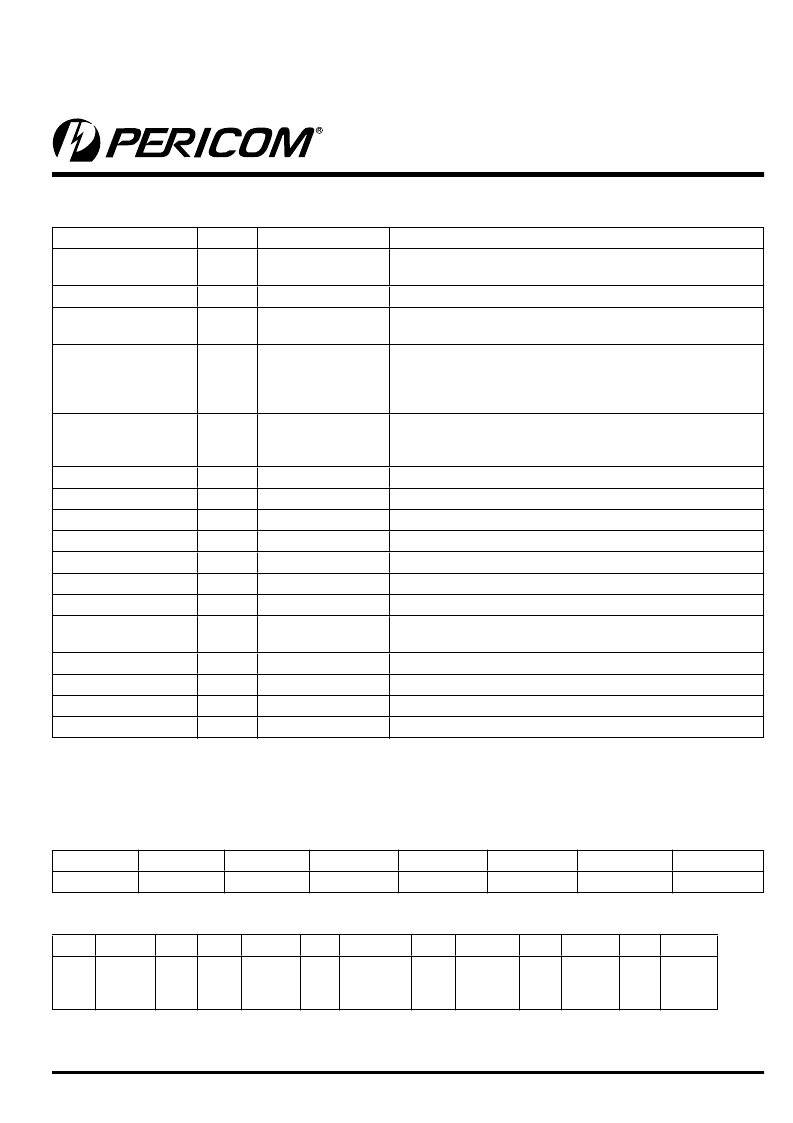
Pin Descriptions
Pin Name
Type
Pin #
Descriptions
SRC_DIV#
Input
1
3.3V LVTTL input for selecting input frequency divide by 2,
active LOW.
0.7V Differential SRC input from PI6C410 clock synthesizer
SRC & SRC#
Input
4, 5
OE [0:7]
Input
6, 7, 14, 15, 35, 36,
43, 44
3.3V LVTTL input for enabling outputs, active HIGH.
OE_INV
Input
40
3.3V LVTTL input for inverting the OE, SRC_STOP# and
PWRDWN# pins.
When 0 = same stage
When 1 = OE[0:7], SRC_STOP#, PWRDWN# inverted.
OUT[0:7] & OUT[0:7]#
Output
8, 9, 12, 13, 16 17,
20, 21, 29, 30, 33, 34,
37, 38, 41, 42
22
23
24
46
27
28
26
0.7V Differential outputs
PLL/BYPASS#
SCLK
SDA
I
REF
SRC_STOP#
PLL_BW#
PWRDWN#
Input
Input
I/O
Input
Input
Input
Input
3.3V LVTTL input for selecting fan-out of PLL operation.
SMBus compatible SCLOCK input
SMBus compatible SDATA
External resistor connection to set the differential output current
3.3V LVTTL input for SRC stop, active LOW
3.3V LVTTL input for selecting the PLL bandwidth
3.3V LVTTL input for Power Down operation, active LOW
3.3V LVTTL output, transition high when PLL lock is achieved
(Latched output)
3.3V Power Supply for Outputs
Ground for Outputs
Ground for PLL
3.3V Power Supply for PLL
LOCK
Output
45
V
DD
V
SS
V
SS_A
V
DD_A
Power
Ground
Ground
Power
2, 11, 19, 31, 39
3, 10, 18, 25, 32
47
48
Serial Data Interface (SMBus)
PI6C20800 is a slave only SMBus device that supports indexed block read and indexed block write protocol using a single 7-bit
address and read/write bit as shown below.
Address assignment
A6
1
A5
1
A4
0
A3
1
A2
1
A1
1
A0
0
R/W
0/1
Data Protocol
(1)
1 bit
7 bits
1
1
8 bits
1
8 bits
Byte
Count
= N
1
8 bits
1
8 bits
Data
Byte N
- 1
1
1 bit
Start
bit
Slave
Addr
R/W
Ack
Register
offset
Ack
Ack
Data
Byte 0
Ack
Ack
Stop
bit
Note:
1.
Register offset for indicating the starting register for indexed block write and indexed block read. Byte Count in write mode cannot be 0.
相关PDF资料 |
PDF描述 |
|---|---|
| PI6C20800AE | 1:8 Clock Driver for Intel PCI Express Chipsets |
| PI6C20800VE | 1:8 Clock Driver for Intel PCI Express Chipsets |
| PI6C210A | CPU SYSTEM CLOCK GENERATOR|CMOS|TSSOP|48PIN|PLASTIC |
| PI6C210V | 8-Channel, Micropower Sampling 12-Bit Serial I/O A/D Converter; Package: SSOP; No of Pins: 24; Temperature Range: -40°C to +85°C |
| PI6C2301W | Clock Driver |
相关代理商/技术参数 |
参数描述 |
|---|---|
| PI6C20800AE | 功能描述:锁相环 - PLL 1:8 PCI Express Clock Driver RoHS:否 制造商:Silicon Labs 类型:PLL Clock Multiplier 电路数量:1 最大输入频率:710 MHz 最小输入频率:0.002 MHz 输出频率范围:0.002 MHz to 808 MHz 电源电压-最大:3.63 V 电源电压-最小:1.71 V 最大工作温度:+ 85 C 最小工作温度:- 40 C 封装 / 箱体:QFN-36 封装:Tray |
| PI6C20800AEX | 功能描述:锁相环 - PLL 1:8 PCI Express Clock Driver RoHS:否 制造商:Silicon Labs 类型:PLL Clock Multiplier 电路数量:1 最大输入频率:710 MHz 最小输入频率:0.002 MHz 输出频率范围:0.002 MHz to 808 MHz 电源电压-最大:3.63 V 电源电压-最小:1.71 V 最大工作温度:+ 85 C 最小工作温度:- 40 C 封装 / 箱体:QFN-36 封装:Tray |
| PI6C20800BAE | 功能描述:时钟缓冲器 1:8 PCI Exp Gen 2/3 Zero Delay Buffer RoHS:否 制造商:Texas Instruments 输出端数量:5 最大输入频率:40 MHz 传播延迟(最大值): 电源电压-最大:3.45 V 电源电压-最小:2.375 V 最大功率耗散: 最大工作温度:+ 85 C 最小工作温度:- 40 C 封装 / 箱体:LLP-24 封装:Reel |
| PI6C20800BAEX | 功能描述:时钟缓冲器 1:8 PCI Exp Gen 2/3 Zero Delay Buffer RoHS:否 制造商:Texas Instruments 输出端数量:5 最大输入频率:40 MHz 传播延迟(最大值): 电源电压-最大:3.45 V 电源电压-最小:2.375 V 最大功率耗散: 最大工作温度:+ 85 C 最小工作温度:- 40 C 封装 / 箱体:LLP-24 封装:Reel |
| PI6C20800BIAE | 功能描述:时钟缓冲器 1:8 PCI Exps Gen2/3 ZeroDelay Buffer Ind RoHS:否 制造商:Texas Instruments 输出端数量:5 最大输入频率:40 MHz 传播延迟(最大值): 电源电压-最大:3.45 V 电源电压-最小:2.375 V 最大功率耗散: 最大工作温度:+ 85 C 最小工作温度:- 40 C 封装 / 箱体:LLP-24 封装:Reel |
发布紧急采购,3分钟左右您将得到回复。