- 您现在的位置:买卖IC网 > PDF目录367962 > PI6C2401W (Pericom Semiconductor Corp.) Phase-Locked Loop Clock Driver PDF资料下载
参数资料
| 型号: | PI6C2401W |
| 厂商: | Pericom Semiconductor Corp. |
| 英文描述: | Phase-Locked Loop Clock Driver |
| 中文描述: | 锁相环时钟驱动器 |
| 文件页数: | 1/4页 |
| 文件大小: | 74K |
| 代理商: | PI6C2401W |
1
PS8419C 01/12/05
1
2
3
AV
CC
4
CLK_OUT
CLK_IN
GND
FB_IN
8
7
6
5
AGND
V
CC
S
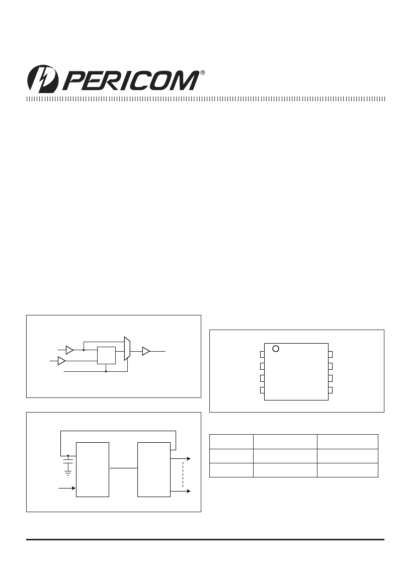
Product Pin Configuration
Logic Block Diagram
12345678901234567890123456789012123456789012345678901234567890121234567890123456789012345678901212345678901234567890123456789012123456789012
12345678901234567890123456789012123456789012345678901234567890121234567890123456789012345678901212345678901234567890123456789012123456789012
PI6C2401
Product Features
High-Performance Phase-Locked-Loop Clock Distribution for
Networking, ATM, 100/134 MHz Registered DIMM Synchro-
nous DRAM modules for server/workstation/PC applications
Zero Input-to-Output delay
Low jitter: Cycle-to-Cycle jitter ± 100ps max.
On-chip series damping resistor at clock output drivers
for low noise and EMI reduction
Operates at 3.3V V
CC
Packaged in Plastic 8-pin SOIC Package (W)
Pb-free and Green Available
Wide range of Clock Frequencies
Phase-Locked Loop Clock Driver
Product Description
The PI6C2401 features a low-skew, low-jitter, phase-locked loop
(PLL) clock driver. By connecting the feedback CLK_OUT
output
to the feedback FB_IN input, the propagation delay from the
CLK_IN input to any clock output will be nearly zero.
Application
If the system designer needs more than 16 outputs with the features
just described, using two or more zero-delay buffers such as
PI6C2509Q, and PI6C2510Q, is likely to be impractical. The device-
to-device skew introduced can significantly reduce
the performance. Pericom recommends the use of a zero-delay
buffer and an eighteen output non-zero-delay buffer . As shown in
Figure 1, this combination produces a zero-delay buffer with all the
signal characteristics of the original zero-delay buffer, but with as
many outputs as the non-zero-delay buffer part. For example, when
combined with an eighteen output non-zero delay buffer, a system
designer can create a seventeen-output zero-delay buffer.
Figure 1. This Combination Provides Zero-Delay Between
the Reference Clocks Signal and 17 Outputs
17
Zero Delay
Buffer
PI6C2401
Reference
Clock
Signal
CLK_OUT
Feedback
18 Output
Non-Zero
Delay
Buffer
V
S
e
u
o
S
t
p
O
n
w
o
d
h
S
L
L
P
1
L
L
P
N
0
N
I
K
L
C
Y
Control Input
CLK_IN
FB_IN
S
PLL
CLK_OUT
8-Pin
W
相关PDF资料 |
PDF描述 |
|---|---|
| PI6C2401WE | Phase-Locked Loop Clock Driver |
| PI6C2404A | Zero-Delay Clock Buffer |
| PI6C2405A-1L | Zero-Delay Clock Buffer |
| PI6C2405A-1LE | Zero-Delay Clock Buffer |
| PI6C2405A-1LI | Zero-Delay Clock Buffer |
相关代理商/技术参数 |
参数描述 |
|---|---|
| PI6C2401WE | 功能描述:锁相环 - PLL 3.3v Zero Delay Clock RoHS:否 制造商:Silicon Labs 类型:PLL Clock Multiplier 电路数量:1 最大输入频率:710 MHz 最小输入频率:0.002 MHz 输出频率范围:0.002 MHz to 808 MHz 电源电压-最大:3.63 V 电源电压-最小:1.71 V 最大工作温度:+ 85 C 最小工作温度:- 40 C 封装 / 箱体:QFN-36 封装:Tray |
| PI6C2401WEX | 功能描述:锁相环 - PLL 3.3v Zero Delay Driver RoHS:否 制造商:Silicon Labs 类型:PLL Clock Multiplier 电路数量:1 最大输入频率:710 MHz 最小输入频率:0.002 MHz 输出频率范围:0.002 MHz to 808 MHz 电源电压-最大:3.63 V 电源电压-最小:1.71 V 最大工作温度:+ 85 C 最小工作温度:- 40 C 封装 / 箱体:QFN-36 封装:Tray |
| PI6C2402 | 制造商:未知厂家 制造商全称:未知厂家 功能描述:Clock IC | 1 Output Zero-Delay Clock Driver w/ Ext. Loopback. 2X Multiplier |
| PI6C2402WE | 功能描述:锁相环 - PLL 3.3v Zero Delay Clock RoHS:否 制造商:Silicon Labs 类型:PLL Clock Multiplier 电路数量:1 最大输入频率:710 MHz 最小输入频率:0.002 MHz 输出频率范围:0.002 MHz to 808 MHz 电源电压-最大:3.63 V 电源电压-最小:1.71 V 最大工作温度:+ 85 C 最小工作温度:- 40 C 封装 / 箱体:QFN-36 封装:Tray |
| PI6C2402WEX | 功能描述:锁相环 - PLL 3.3v Zero Delay Driver RoHS:否 制造商:Silicon Labs 类型:PLL Clock Multiplier 电路数量:1 最大输入频率:710 MHz 最小输入频率:0.002 MHz 输出频率范围:0.002 MHz to 808 MHz 电源电压-最大:3.63 V 电源电压-最小:1.71 V 最大工作温度:+ 85 C 最小工作温度:- 40 C 封装 / 箱体:QFN-36 封装:Tray |
发布紧急采购,3分钟左右您将得到回复。