参数资料
| 型号: | PI74FCT245TQEX |
| 厂商: | Pericom |
| 文件页数: | 2/7页 |
| 文件大小: | 0K |
| 描述: | IC TXRX OCTAL BIDIR 20QSOP |
| 标准包装: | 3,000 |
| 系列: | 74FCT |
| 逻辑类型: | 收发器,非反相 |
| 元件数: | 1 |
| 每个元件的位元数: | 8 |
| 输出电流高,低: | 15mA,64mA |
| 电源电压: | 4.75 V ~ 5.25 V |
| 工作温度: | -40°C ~ 85°C |
| 安装类型: | 表面贴装 |
| 封装/外壳: | 20-SSOP(0.154",3.90mm 宽) |
| 供应商设备封装: | 20-QSOP |
| 包装: | 带卷 (TR) |
2
PS2012E
08/08/06
12345678901234567890123456789012123456789012345678901234567890121234567890123456789012345678901212345678901234567890123456789012123456789012
PI74FCT245T
PI74FCT2245T(25 Ohm Series )
Octal BidirectionalTransceivers
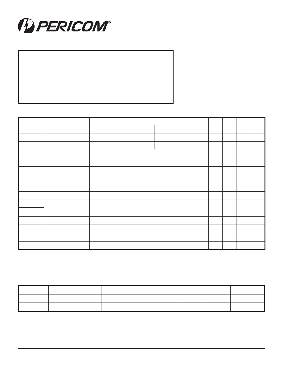
Storage Temperature .................................................................... –65°Cto+150°C
Ambient Temperature with Power Applied .................................... –40°Cto+85°C
Supply Voltage to Ground Potential (Inputs & VCC Only) ............. –0.5Vto+7.0V
Supply Voltage to Ground Potential (Outputs & D/O Only) ........... –0.5Vto+7.0V
DC Input Voltage ............................................................................ –0.5Vto+7.0V
DC Output Current ...................................................................................... 120mA
Power Dissipation ..........................................................................................0.5W
Note:
Stresses greater than those listed under MAXIMUM
RATINGS may cause permanent damage to the device.
This is a stress rating only and functional operation
of the device at these or any other conditions above
those indicated in the operational sections of this
specification is not implied. Exposure to absolute
maximum rating conditions for extended periods may
affect reliability.
DC Electrical Characteristics (Over the Operating Range, TA = –40°C to +85°C, VCC = 5.0V ±5%)
Parameters Description
Test Conditions(1)
Min. Typ(2) Max.
Units
VOH
Output HIGH Voltage
VCC = Min., VIN = VIH or VIL
IOH =–15.0mA
2.4
3.0
V
VOL
Output LOW Current
VCC = Min., VIN = VIH or VIL
IOL = 64mA
0.3
0.55
V
VOL
Output LOW Current
VCC = Min., VIN = VIH or VIL
IOL = 12mA (25
Ω Series)
0.3
0.50
V
VIH
Input HIGH Voltage
Guaranteed Logic HIGH Level
2.0
V
VIL
Input LOW Voltage
Guaranteed Logic LOW Level
0.8
V
IIH
Input HIGH Current
(Except I/O pins) VCC = Max.
VIN=VCC
1
μA
IIL
Input LOW Current
(Except I/O pins) VCC = Max.
VIN=GND
–1
μA
IIH
Input HIGH Current
(I/O pins Only) VCC = Max.
VIN=VCC
1
μA
IIL
Input LOW Current
(I/O pins Only) VCC = Max.
VIN=GND
–1
μA
IOZH
High Impedance
VCC = MAX.VOUT =2.7V
1
μA
IOZL
Output Current
VOUT=0.5V
–1
μA
VIK
Clamp Diode Voltage
VCC = Min., IIN = –18 mA
–0.7
–1.2
V
IOFF
Power Down Disable
VCC=GND,VOUT=4.5V
100
μA
IOS
Short Circuit Current
VCC= Max.(3), VOUT = GND
–60
–120
mA
VH
Input Hysteresis
200
mV
Capacitance (TA = 25°C, f = 1 MHz)
Parameters
(1)
Description
Test Conditions
Typ.
Max.
Units
CIN
Input Capacitance
VIN=0V
6
10
pF
COUT
Output Capacitance
VOUT = 0V
8
12
pF
Notes:
1. These Parameters are determined by device characterization but are not production tested.
Maximum Ratings
(Above which the useful life may be impaired. For user guidelines, not tested.)
Notes:
1. For Max. or Min. conditions, use appropriate value specified under Electrical Characteristics for the applicable device type.
2. Typical values are at VCC = 5.0V, +25°C ambient and maximum loading.
3. Not more than one output should be shorted at one time. Duration of the test should not exceed one second.
06-0207
相关PDF资料 |
PDF描述 |
|---|---|
| MC14526BDWG | IC COUNTER BINARY 6BIT 16-SOIC |
| 74VHC393SJ | IC COUNTER BIN DUAL 4BIT 14SOP |
| 74VHC161SJ | IC COUNTER BINARY 4BIT 16SOP |
| MC14526BDWR2G | IC COUNTER BINARY 6BIT 16-SOIC |
| OSTEH182160 | CONN TERM BLOCK 18POS 3.5MM |
相关代理商/技术参数 |
参数描述 |
|---|---|
| PI74FCT245TQX | 制造商:Pericom Semiconductor Corporation 功能描述:Bus XCVR Single 8-CH 3-ST 20-Pin QSOP T/R |
| PI74FCT245TS | 制造商:PERI 功能描述: |
| PI74FCT245TSA | 制造商:Pericom Semiconductor Corporation 功能描述:Bus Transceiver, Single, 8 Bit, 20 Pin, Plastic, SOP |
| PI74FCT245TSE | 功能描述:总线收发器 Octal Bidirectional Transceiver RoHS:否 制造商:Fairchild Semiconductor 逻辑类型:CMOS 逻辑系列:74VCX 每芯片的通道数量:16 输入电平:CMOS 输出电平:CMOS 输出类型:3-State 高电平输出电流:- 24 mA 低电平输出电流:24 mA 传播延迟时间:6.2 ns 电源电压-最大:2.7 V, 3.6 V 电源电压-最小:1.65 V, 2.3 V 最大工作温度:+ 85 C 封装 / 箱体:TSSOP-48 封装:Reel |
| PI74FCT245TSEX | 功能描述:总线收发器 Octal Bidirectional Transceiver RoHS:否 制造商:Fairchild Semiconductor 逻辑类型:CMOS 逻辑系列:74VCX 每芯片的通道数量:16 输入电平:CMOS 输出电平:CMOS 输出类型:3-State 高电平输出电流:- 24 mA 低电平输出电流:24 mA 传播延迟时间:6.2 ns 电源电压-最大:2.7 V, 3.6 V 电源电压-最小:1.65 V, 2.3 V 最大工作温度:+ 85 C 封装 / 箱体:TSSOP-48 封装:Reel |
发布紧急采购,3分钟左右您将得到回复。