- 您现在的位置:买卖IC网 > PDF目录368011 > PI74FCT280BT (Pericom Semiconductor Corp.) Fast CMOS 9-Bit Parity Generator/Checker PDF资料下载
参数资料
| 型号: | PI74FCT280BT |
| 厂商: | Pericom Semiconductor Corp. |
| 英文描述: | Fast CMOS 9-Bit Parity Generator/Checker |
| 中文描述: | 快速CMOS 9位奇偶发生器/检查 |
| 文件页数: | 2/4页 |
| 文件大小: | 39K |
| 代理商: | PI74FCT280BT |
PI74FCT280T
9-BIT PARITY GENERATOR/CHECKER
2
PS2014A 03/11/96
12345678901234567890123456789012123456789012345678901234567890121234567890123456789012345678901212345678901234567890123456789012123456789012
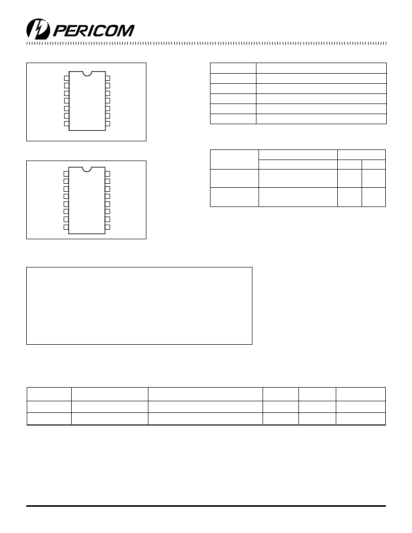
PI74FCT280T 14-Pin SOIC Configuration
Inputs
I
8
-I
0
Outputs
Σ
e
H
Function
Even Parity
Σ
o
L
No. of Bits at TTL High
= 0, 2, 4, 6, 8
No. of Bits at TTL High
= 1, 3, 5, 7, 9
Odd Parity
L
H
Truth Table
(1)
Note:
1.
H = High Voltage Level
L = Low Voltage Level
Pin Name
I
8
–I
0
Σ
e
Σ
o
GND
V
CC
Description
Data In
Even Parity Out
Odd Parity Out
Ground
Power
Product Pin Description
Maximum Ratings
(Above which the useful life may be impaired. For user guidelines, not tested.)
Storage Temperature ................................................................. –65°C to +150°C
Ambient Temperature with Power Applied .................................-40°C to +85°C
Supply Voltage to Ground Potential (Inputs & Vcc Only) ..........–0.5V to +7.0V
Supply Voltage to Ground Potential (Outputs & D/O Only) ...........–0.5V +7.0V
DC Input Voltage .........................................................................–0.5V to +7.0V
DC Output Current ................................................................................... 120 mA
Power Dissipation......................................................................................... 0.5W
Note:
Stresses greater than those listed under
MAXIMUM RATINGS may cause permanent
damage to the device. This is a stress rating
only and functional operation of the device at
these or any other conditions above those
indicated in the operational sections of this
specification is not implied. Exposure to
absolute maximum rating conditions for
extended periods may affect reliability.
Capacitance
(T
A
= 25°C, f = 1 MHz)
Parameters
(1)
Description
Test Conditions
Typ
Max.
Units
C
IN
Input Capacitance
V
IN
= 0V
6
10
pF
C
OUT
Output Capacitance
V
OUT
= 0V
8
12
pF
Notes:
1. This parameter is determined by device characterization but is not production tested.
PI74FCT280T 16-Pin QSOP Configuration
V
CC
I
5
I
4
I
3
I
2
I
1
I
0
1
2
3
4
5
6
7
I
6
I
7
14
13
12
11
10
9
8
NC
I
8
Σ
e
Σ
o
GND
14-PIN
W14
V
CC
I
5
I
4
I
3
I
2
I
1
I
0
NC
1
2
3
4
5
6
7
I
6
I
7
16
15
14
13
12
11
10
NC
I
8
Σ
e
Σ
o
NC
8
GND
9
16-PIN
Q16
相关PDF资料 |
PDF描述 |
|---|---|
| PI74FCT280CT | Fast CMOS 9-Bit Parity Generator/Checker |
| PI74FCT280T | Fast CMOS 9-Bit Parity Generator/Checker |
| PI74FCT2827T | Fast CMOS 10-Bit Buffers |
| PI74FCT2828T | Fast CMOS 10-Bit Buffers |
| PI74FCT827T | Fast CMOS 10-Bit Buffers |
相关代理商/技术参数 |
参数描述 |
|---|---|
| PI74FCT2821TSA | 制造商:Pericom Semiconductor Corporation 功能描述: |
| PI74FCT2827ATP | 制造商:Pericom Semiconductor Corporation 功能描述:Buffer/Line Driver 10-CH Non-Inverting 3-ST CMOS 24-Pin PDIP Tube |
| PI74FCT2827ATQ | 功能描述:IC BUFFER 10BIT NON-INV 24QSOP RoHS:否 类别:集成电路 (IC) >> 逻辑 - 缓冲器,驱动器,接收器,收发器 系列:74FCT 标准包装:1,000 系列:74ABT 逻辑类型:寄存收发器,非反相 元件数:1 每个元件的位元数:8 输出电流高,低:32mA,64mA 电源电压:4.5 V ~ 5.5 V 工作温度:-40°C ~ 85°C 安装类型:表面贴装 封装/外壳:24-SOIC(0.295",7.50mm 宽) 供应商设备封装:24-SOIC 包装:带卷 (TR) |
| PI74FCT2827ATS | 制造商:Pericom Semiconductor Corporation 功能描述: |
| PI74FCT2827TQB | 制造商:Pericom Semiconductor Corporation 功能描述: |
发布紧急采购,3分钟左右您将得到回复。