- 您现在的位置:买卖IC网 > PDF目录368011 > PI74FCT3245 (Pericom Semiconductor Corp.) Fast CMOS 3.3V 8-Bit Bidirectional Transceiver PDF资料下载
参数资料
| 型号: | PI74FCT3245 |
| 厂商: | Pericom Semiconductor Corp. |
| 英文描述: | Fast CMOS 3.3V 8-Bit Bidirectional Transceiver |
| 中文描述: | 快速CMOS 3.3V的8位双向收发器 |
| 文件页数: | 2/4页 |
| 文件大小: | 44K |
| 代理商: | PI74FCT3245 |
PI74FCT3245
3.3V 8-BIT BIDIRECTIONAL TRANSCEIVER
2
PS7068C 8/22/97
12345678901234567890123456789012123456789012345678901234567890121234567890123456789012345678901212345678901234567890123456789012123456789012
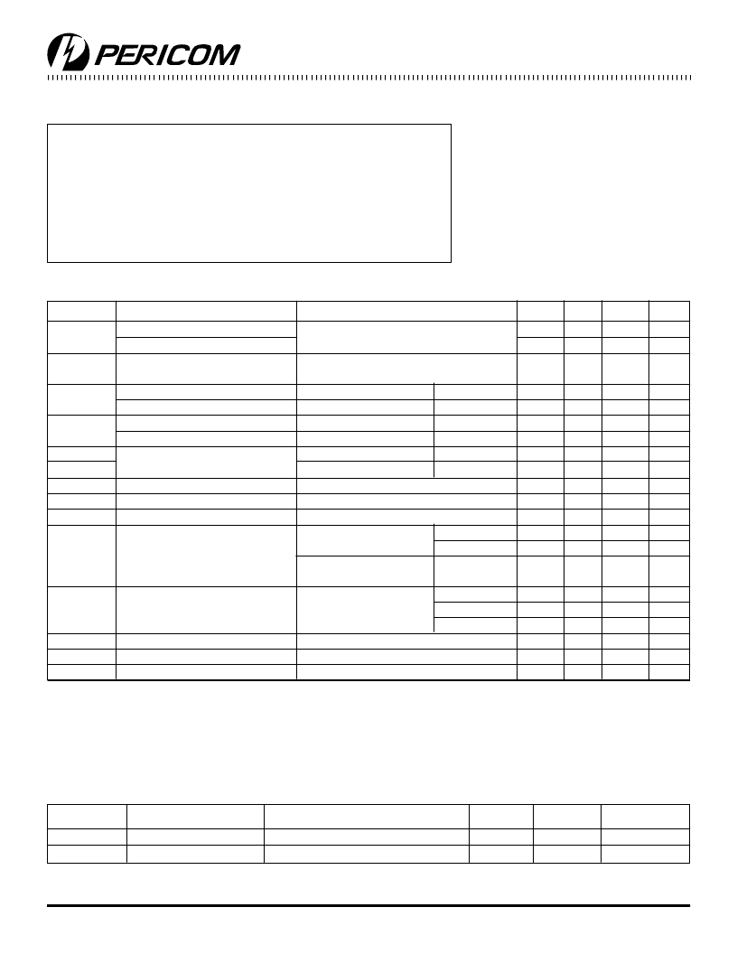
Storage Temperature.................................................................. –65°C to +150°C
Ambient Temperature with Power Applied................................. –40°C to +85°C
Supply Voltage to Ground Potential (Inputs & Vcc Only)...........–0.5V to +7.0V
Supply Voltage to Ground Potential (Outputs & D/O Only) .......–0.5V to +7.0V
DC Input Voltage .........................................................................–0.5V to +7.0V
DC Output Current ....................................................................................120mA
Power Dissipation......................................................................................... 1.0W
Note:
Stresses greater than those listed under
MAXIMUM RATINGS may cause permanent
damage to the device. This is a stress rating
only and functional operation of the device at
these or any other conditions above those indi-
cated in the operational sections of this specifi-
cation is not implied. Exposure to absolute
maximum rating conditions for extended peri-
ods may affect reliability.
DC Electrical Characteristics
(Over the Operating Range, T
A
= –40°C to +85°C, V
CC
= 2.7V to 3.6V)
Parameters
V
IH
Description
Test Conditions
(1)
Min.
2.2
2.0
–0.5
Typ.
(2)
—
—
—
Max.
5.5
5.5
0.8
Units
V
V
V
Input HIGH Voltage (Input pins)
Input HIGH Voltage (I/O pins)
Input LOW Voltage
(Input and I/O pins)
Input HIGH Current (Input pins)
Input HIGH Current (I/O pins)
Input LOW Current (Input pins)
Input LOW Current (I/O pins)
High Impedance Output Current
(3-State Output pins)
Clamp Diode Voltage
Output HIGH Current
Output LOW Current
Output HIGH Voltage
Guaranteed Logic HIGH Level
V
IL
Guaranteed Logic LOW Level
I
IH
V
CC
= Max.
V
CC
= Max.
V
CC
= Max.
V
CC
= Max.
V
CC
= Max.
V
CC
= Max.
V
CC
= Min., I
IN
= –18 mA
V
CC
= 3.3V, V
IN
= V
IH
or V
IL
, V
O
= 1.5V
(3)
–36
V
CC
= 3.3V, V
IN
= V
IH
or V
IL
, V
O
= 1.5V
(3)
50
V
CC
= Min.
V
IN
= V
IH
or V
IL
V
CC
= 3.0V,
V
IN
= V
IH
or V
IL
V
CC
= Min.
V
IN
= V
IH
or V
IL
V
IN
= 5.5V
V
IN
= V
CC
V
IN
= GND
V
IN
= GND
V
OUT
= 5.5V
V
OUT
= GND
—
—
—
—
—
—
—
—
—
—
—
—
—
–0.7
–60
90
—
3.0
3.0
—
—
0.2
0.3
–85
—
150
±1
±1
±1
±1
±1
±1
–1.2
–110
200
—
—
—
—
0.2
0.4
0.5
–240
±100
—
μA
μA
μA
μA
μA
μA
V
mA
mA
V
V
V
I
IL
I
OZH
I
OZL
V
IK
I
ODH
I
ODL
V
OH
I
OH
= –0.1 mA Vcc-0.2
I
OH
= –3 mA
I
OH
= –8 mA
I
OH
= –24 mA
I
OL
= 0.1 mA
I
OL
= 16 mA
I
OL
= 24 mA
2.4
2.4
(5)
2.0
—
—
—
–60
—
—
V
OL
Output LOW Voltage
V
V
V
I
OS
I
OFF
V
H
Short Circuit Current
(4)
Power Down Disable
Input Hysteresis
V
CC
= Max.
(3)
, V
OUT
= GND
V
CC
= 0V, V
IN
or V
OUT
≤
4.5V
mA
μA
mV
Capacitance
(T
A
= 25°C, f = 1 MHz)
Parameters
(1)
C
IN
C
OUT
Note:
1. This parameter is determined by device characterization but is not production tested.
Description
Input Capacitance
Output Capacitance
Test Conditions
V
IN
= 0V
V
OUT
= 0V
Typ.
4.5
5.5
Max.
6
8
Units
pF
pF
Notes:
1. For Max. or Min. conditions, use appropriate value specified under Electrical Characteristics for the applicable device type.
2. Typical values are at Vcc = 3.3V, +25°C ambient and maximum loading.
3. Not more than one output should be shorted at one time. Duration of the test should not exceed one second.
4. This parameter is guaranteed but not tested.
5. V
OH
= V
CC
– 0.6V at rated current.
Maximum Ratings
(Above which the useful life may be impaired. For user guidelines, not tested.)
相关PDF资料 |
PDF描述 |
|---|---|
| PI74FCT3573 | Fast CMOS 3.3V 8-Bit Transparent Latch |
| PI74FCT373T | Fast CMOS Octal Transparent Latches |
| PI74FCT573ATH | Fast CMOS Octal Transparent Latches |
| PI74FCT573ATL | Fast CMOS Octal Transparent Latches |
| PI74FCT573ATQ | Fast CMOS Octal Transparent Latches |
相关代理商/技术参数 |
参数描述 |
|---|---|
| PI74FCT3245CSX | 制造商:PERICOM 功能描述: |
| PI74FCT373ATQ | 功能描述:IC OCT TRANSPARENT LATCH 20 QSOP RoHS:否 类别:集成电路 (IC) >> 逻辑 - 锁销 系列:74FCT 产品变化通告:Product Discontinuation 09/Dec/2010 标准包装:1,500 系列:74VCX 逻辑类型:D 型透明锁存器 电路:8:8 输出类型:三态 电源电压:1.8 V ~ 3.6 V 独立电路:2 延迟时间 - 传输:1.5ns 输出电流高,低:6mA,6mA 工作温度:-40°C ~ 85°C 安装类型:表面贴装 封装/外壳:48-TFSOP(0.240",6.10mm 宽) 供应商设备封装:48-TSSOP 包装:带卷 (TR) |
| PI74FCT373ATQE | 功能描述:闭锁 Octal Transparent 闭锁 RoHS:否 制造商:Micrel 电路数量:1 逻辑类型:CMOS 逻辑系列:TTL 极性:Non-Inverting 输出线路数量:9 高电平输出电流: 低电平输出电流: 传播延迟时间: 电源电压-最大:12 V 电源电压-最小:5 V 最大工作温度:+ 85 C 最小工作温度:- 40 C 封装 / 箱体:SOIC-16 封装:Reel |
| PI74FCT373ATQEX | 功能描述:闭锁 Octal Transparent 闭锁 RoHS:否 制造商:Micrel 电路数量:1 逻辑类型:CMOS 逻辑系列:TTL 极性:Non-Inverting 输出线路数量:9 高电平输出电流: 低电平输出电流: 传播延迟时间: 电源电压-最大:12 V 电源电压-最小:5 V 最大工作温度:+ 85 C 最小工作温度:- 40 C 封装 / 箱体:SOIC-16 封装:Reel |
| PI74FCT373ATQX | 制造商:Pericom Semiconductor Corporation 功能描述:Latch Transparent 3-ST 8-CH D-Type 20-Pin QSOP T/R |
发布紧急采购,3分钟左右您将得到回复。