参数资料
| 型号: | PI74SSTVF16859AZBE |
| 厂商: | Pericom |
| 文件页数: | 1/8页 |
| 文件大小: | 0K |
| 描述: | IC REG BUFFER 13-26BIT 56-QFN |
| 产品变化通告: | Product Discontinuation Notice 11/Feb/2008 |
| 标准包装: | 348 |
| 系列: | 74SSTVF |
| 逻辑类型: | 13 位至 26 位寄存缓冲器,DDR |
| 电源电压: | 2.3 V ~ 2.7 V |
| 位数: | 13,26 |
| 工作温度: | 0°C ~ 70°C |
| 安装类型: | 表面贴装 |
| 封装/外壳: | 56-VFQFN 裸露焊盘 |
| 供应商设备封装: | 56-QFN-EP(8x8) |
| 包装: | 托盘 |
1
PS8684B
10/30/06
Product Description
Pericom Semiconductor’s PI74SSTVF16859A logic circuit is
produced using the Company’s advanced sub-micron CMOS
technology, achieving industry leading speed.
All inputs are compatible with the JEDEC standard for SSTL_2,
except the LVCMOS reset (RESET) input. All outputs are SSTL_2,
Class II compatible.
The device operates from a differential clock (CLK and CLK). Data
registered at the crossing of CLK going HIGH, and CLK going LOW.
The PI74SSTVF16859A supports low-power standby operation.
When RESET is LOW, the differential input receivers are disabled,
and undriven (floating) data, clock and reference voltage (VREF)
inputs are allowed. In addition, when RESET is LOW, all registers are
reset, and all outputs are forced LOW. The LVCMOS RESET input
must always be held at a valid logic HIGH or LOW level.
To ensure defined outputs from the register before a stable clock
has been supplied, RESET must be held in the LOW state during
power up.
In the DDR DIMM application, RESET is specified to be completely
asynchronous with respect to CLK and CLK. Therefore, no timing
relationship can be guaranteed between the two. When entering
RESET, the register will be cleared and the outputs will be driven
LOW quickly, relative to the time to disable the differential input
receivers, thus ensuring no glitches on the output. However, when
coming out of RESET, the register will become active quickly, relative
to the time to enable the differential input receivers. When the data
inputs are LOW, and the clock is stable, during the time from the
LOW-to-HIGH transition of RESET until the input receivers
are fully enabled, the design must ensure that the outputs will
remainLOW.
Pericom’s PI74SSTVF16859A is characterized for operation from
0°C to 70°C.
Product Features
PI74 SSTVF16859A is designed for low-voltage operation,
2.5V for PC1600 ~ PC2700; 2.6V for PC3200
Supports SSTL_2 Class I specifications on outputs
All Inputs are SSTL_2 Compatible, except RESET
which is LVCMOS.
Designed for DDR Memory
Flow-Through Architecture
Package: 56-pin, Plastic Very Thin Fine Pitch Quad Flat No-
Lead QFN (ZB). (Pb-free available)
Product Pin Description
13-Bit to 26-Bit Registered Buffer
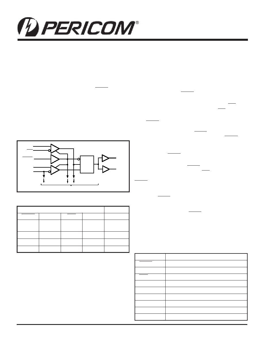
Logic Block Diagram
TO 12 OTHER CHANNELS
RESET
CLK
35
36
VREF
D1
24
32
D
R
CLK
Q1A
7
Q1B
22
CLK
V
38
s
t
u
p
n
Is
t
u
p
t
u
O
T
E
S
E
RK
L
CK
L
CD
Q
L
r
o
X
g
n
i
t
a
o
l
F
r
o
X
g
n
i
t
a
o
l
F
r
o
X
g
n
i
t
a
o
l
F
L
H
↑↓
HH
Η↑
↓
LL
HH
r
o
LH
r
o
LX
o
Q
)
2
(
Truth Table(1)
Notes:
1. H = High Signal Level
L
= Low Signal Level
↑ = Transition LOW-to-HIGH
↓ = Transition HIGH-to-LOW
X = Irrelevant or floating
2. Output level before the
indicated steady state
input conditions were
established.
e
m
a
N
n
i
Pn
o
i
t
p
i
r
c
s
e
D
T
E
S
E
RS
O
M
C
V
L
)
w
o
L
e
v
i
t
c
A
(
t
e
s
e
R
K
L
Ct
u
p
n
I
l
a
i
t
n
e
r
e
f
i
D
e
v
i
t
i
s
o
P
,
t
u
p
n
I
k
c
o
l
C
K
L
Ct
u
p
n
I
l
a
i
t
n
e
r
e
f
i
D
e
v
i
t
a
g
e
N
,
t
u
p
n
I
k
c
o
l
C
D3
1
D
-
1
D
,
t
u
p
n
I
a
t
a
D
Q3
1
Q
-
1
Q
,
t
u
p
t
u
O
a
t
a
D
N
Gd
n
u
o
r
G
V D
D
e
g
a
t
l
o
V
y
l
p
u
S
e
r
o
C
V
Q
D
e
g
a
t
l
o
V
y
l
p
u
S
t
u
p
t
u
O
V
F
E
R
e
g
a
t
l
o
V
e
c
n
e
r
e
f
e
R
t
u
p
n
I
PI74SSTVF16859A
06-0288
相关PDF资料 |
PDF描述 |
|---|---|
| PI74STX1G02CX | IC SINGLE 2-IN NOR GATE SC70-5 |
| PI74STX1GU04CEX | IC UNBUFFERED INVERTER SC70-5 |
| PI74STX4G4245ZJEX | IC 2BIT LVL SHFT BUF/TXRX 16TDFN |
| PI90LVB16L | IC CLOCK BUFFER MUX 1:6 24-TSSOP |
| PI90LVT14QE | IC CLOCK BUFFER MUX 2:5 20-QSOP |
相关代理商/技术参数 |
参数描述 |
|---|---|
| PI74SSTVF16859AZBEX | 制造商:Pericom Semiconductor Corporation 功能描述:Registered Buffer Single 13-CH CMOS 56-Pin TQFN EP T/R |
| PI74SSTVF32852ANBE | 功能描述:寄存器 24B to 48B Registered RoHS:否 制造商:NXP Semiconductors 逻辑类型:CMOS 逻辑系列:HC 电路数量:1 最大时钟频率:36 MHz 传播延迟时间: 高电平输出电流:- 7.8 mA 低电平输出电流:7.8 mA 电源电压-最大:6 V 最大工作温度:+ 125 C 封装 / 箱体:SOT-38 封装:Tube |
| PI74SSTVF32852ANBEX | 功能描述:寄存器 24B to 48B Registered RoHS:否 制造商:NXP Semiconductors 逻辑类型:CMOS 逻辑系列:HC 电路数量:1 最大时钟频率:36 MHz 传播延迟时间: 高电平输出电流:- 7.8 mA 低电平输出电流:7.8 mA 电源电压-最大:6 V 最大工作温度:+ 125 C 封装 / 箱体:SOT-38 封装:Tube |
| PI74SSTVF32852NBEX | 制造商:Pericom Semiconductor Corporation 功能描述:Registered Buffer Single 24-CH CMOS 114-Pin LFBGA T/R 制造商:Pericom Semiconductor Corporation 功能描述:IC, POSITIVE EDGE TRIGGERED D FLIP-FLOP, TRUE OUTPUT, PBGA114 |
| PI74SSTVF32852NBX | 制造商:Pericom Semiconductor Corporation 功能描述:REGISTERED BFFR SGL 24-CH CMOS 114LFBGA - Tape and Reel |
发布紧急采购,3分钟左右您将得到回复。