参数资料
| 型号: | PI74VCX16373AE |
| 厂商: | Pericom |
| 文件页数: | 1/8页 |
| 文件大小: | 0K |
| 描述: | IC 16-BIT TRANSP LATCH 48-TSSOP |
| 产品变化通告: | Product Discontinuation 09/Dec/2010 |
| 标准包装: | 39 |
| 系列: | 74VCX |
| 逻辑类型: | D 型透明锁存器 |
| 电路: | 8:8 |
| 输出类型: | 三态 |
| 电源电压: | 1.8 V ~ 3.6 V |
| 独立电路: | 2 |
| 延迟时间 - 传输: | 1.5ns |
| 输出电流高,低: | 6mA,6mA |
| 工作温度: | -40°C ~ 85°C |
| 安装类型: | 表面贴装 |
| 封装/外壳: | 48-TFSOP(0.240",6.10mm 宽) |
| 供应商设备封装: | 48-TSSOP |
| 包装: | 管件 |
1
PS8326C
10/27/06
Description
Pericom Semiconductor’s PI74VCX16373 is particularly suitable
for implementing buffer registers, I/O ports, bidirectional bus
drivers, and working registers. This device can be used as two 8-
bit latches or one 16-bit latch. When the Latch Enable (LE) input
is HIGH, the Q outputs follow the (D) inputs. When LE is taken
LOW, the Q outputs are latched at the levels set up at the D inputs.
A buffered Output Enable (OE) input can be used to place the eight
outputs in either a normal logic state (high or low logic levels) or
a high-impedance state in which the outputs neither load nor drive
the bus lines significantly. The high-impedance state and the
increased drive provide the capability to drive bus lines without
need for interface or pullup components. OE does not affect
internal operations of the latch. Old data can be retained or new
data can be entered while the outputs are in the high impedance
state.
To ensure the high-impedance state during power up or power
down, OE should be tied to VDD through a pullup resistor; the
minimum value of the resistor is determined by the current-sinking
capability of the driver.
The PI74VCX family is I/O Tolerant, allowing it to operate in
mixed 1.8V/3.6V systems.
12345678901234567890123456789012123456789012345678901234567890121234567890123456789012345678901212345678901234567890123456789012123456789012
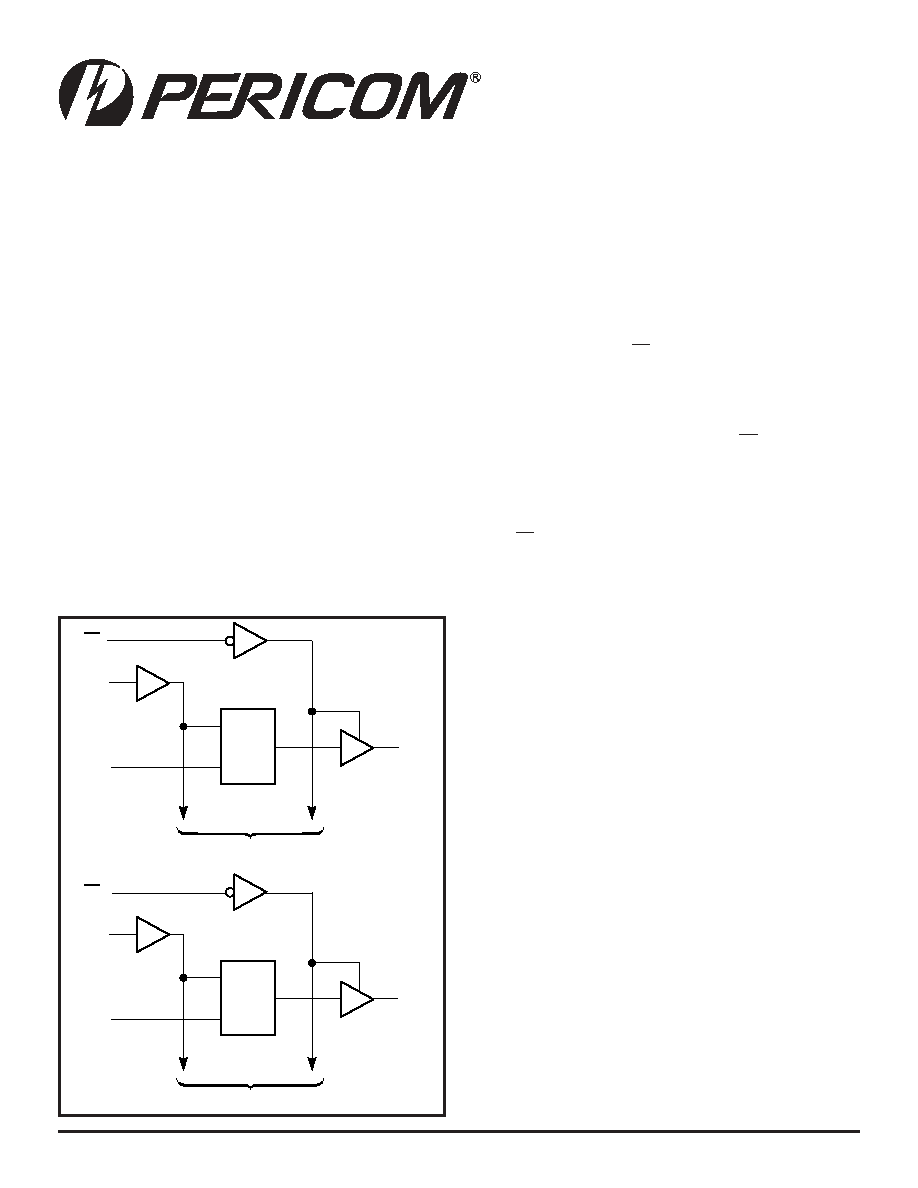
PI74VCX16373
16-Bit Transparent D-Type Latch
with 3-State Outputs
Block Diagram
1LE
1Q1
1D
C1
1D1
To Seven Other Channels
1OE
1
48
47
2
2LE
2Q1
1D
C1
2D1
To Seven Other Channels
25
36
13
24
2OE
Features
The PI74VCX Family is designed for low voltage
operation, VDD = 1.8V to 3.6V
3.6V I/O Tolerant Inputs and Outputs
Supports Live Insertion
Balanced Drive, ±24mA
Uses patented Noise Reduction Circuitry
Typical VOLP (Output Ground Bounce)
< 0.6V at VDD = 2.5V, TA = 25C
Typical VOHV (Output VOH Undershoot)
< –0.6V at VDD = 2.5V, TA = 25C
Power-Off high impedance inputs and outputs
Industrial operation at –40°C to +85°C
Packaging(Pb-free&Greenavailable):
– 48-pin 240-mil wide plastic TSSOP (A)
06-0203
相关PDF资料 |
PDF描述 |
|---|---|
| 74LVT16244BDGVRE4 | IC BUFF/DVR TRI-ST 16BIT 48TVSOP |
| 74LVT16244BDGGRG4 | IC BUFF/DVR TRI-ST 16BIT 48TSSOP |
| PI74FCT373ATQE | IC OCT TRANSPARENT LATCH 20 QSOP |
| MM74HCT373SJX | IC LATCH OCTAL D-TYPE 20-SOP |
| MM74HCT573N | IC LATCH OCTAL D 3STATE 20-DIP |
相关代理商/技术参数 |
参数描述 |
|---|---|
| PI74VCX16373AEX | 功能描述:闭锁 16B Buffer/Line Driver RoHS:否 制造商:Micrel 电路数量:1 逻辑类型:CMOS 逻辑系列:TTL 极性:Non-Inverting 输出线路数量:9 高电平输出电流: 低电平输出电流: 传播延迟时间: 电源电压-最大:12 V 电源电压-最小:5 V 最大工作温度:+ 85 C 最小工作温度:- 40 C 封装 / 箱体:SOIC-16 封装:Reel |
| PI74VCX16374A | 功能描述:IC 16-BIT FLIP-FLOP 48-TSSOP RoHS:否 类别:集成电路 (IC) >> 逻辑 - 触发器 系列:74VCX 产品变化通告:Product Discontinuation 27/Jan/2012 标准包装:2,000 系列:74LCX 功能:标准 类型:D 型总线 输出类型:三态非反相 元件数:1 每个元件的位元数:8 频率 - 时钟:150MHz 延迟时间 - 传输:1.5ns 触发器类型:正边沿 输出电流高,低:24mA,24mA 电源电压:2 V ~ 3.6 V 工作温度:-40°C ~ 85°C 安装类型:表面贴装 封装/外壳:20-SOIC(0.209",5.30mm 宽) 包装:带卷 (TR) 其它名称:MC74LCX574MELG-NDMC74LCX574MELGOSTR |
| PI74VCX16374AE | 功能描述:触发器 16B Edge Trigered D type RoHS:否 制造商:Texas Instruments 电路数量:2 逻辑系列:SN74 逻辑类型:D-Type Flip-Flop 极性:Inverting, Non-Inverting 输入类型:CMOS 输出类型: 传播延迟时间:4.4 ns 高电平输出电流:- 16 mA 低电平输出电流:16 mA 电源电压-最大:5.5 V 最大工作温度:+ 85 C 安装风格:SMD/SMT 封装 / 箱体:X2SON-8 封装:Reel |
| PI74VCX16374AEX | 功能描述:触发器 16B Edge Trigered D type RoHS:否 制造商:Texas Instruments 电路数量:2 逻辑系列:SN74 逻辑类型:D-Type Flip-Flop 极性:Inverting, Non-Inverting 输入类型:CMOS 输出类型: 传播延迟时间:4.4 ns 高电平输出电流:- 16 mA 低电平输出电流:16 mA 电源电压-最大:5.5 V 最大工作温度:+ 85 C 安装风格:SMD/SMT 封装 / 箱体:X2SON-8 封装:Reel |
| PI76850 | 制造商:Texas Instruments 功能描述: |
发布紧急采购,3分钟左右您将得到回复。