- 您现在的位置:买卖IC网 > PDF目录11641 > PIC10F220-E/OT (Microchip Technology)IC PIC MCU FLASH 256X12 SOT-23-6 PDF资料下载
参数资料
| 型号: | PIC10F220-E/OT |
| 厂商: | Microchip Technology |
| 文件页数: | 18/86页 |
| 文件大小: | 0K |
| 描述: | IC PIC MCU FLASH 256X12 SOT-23-6 |
| 标准包装: | 3,000 |
| 系列: | PIC® 10F |
| 核心处理器: | PIC |
| 芯体尺寸: | 8-位 |
| 速度: | 8MHz |
| 外围设备: | POR,WDT |
| 输入/输出数: | 4 |
| 程序存储器容量: | 384B(256 x 12) |
| 程序存储器类型: | 闪存 |
| RAM 容量: | 16 x 8 |
| 电压 - 电源 (Vcc/Vdd): | 2 V ~ 5.5 V |
| 数据转换器: | A/D 2x8b |
| 振荡器型: | 内部 |
| 工作温度: | -40°C ~ 125°C |
| 封装/外壳: | SOT-23-6 |
| 包装: | 散装 |
第1页第2页第3页第4页第5页第6页第7页第8页第9页第10页第11页第12页第13页第14页第15页第16页第17页当前第18页第19页第20页第21页第22页第23页第24页第25页第26页第27页第28页第29页第30页第31页第32页第33页第34页第35页第36页第37页第38页第39页第40页第41页第42页第43页第44页第45页第46页第47页第48页第49页第50页第51页第52页第53页第54页第55页第56页第57页第58页第59页第60页第61页第62页第63页第64页第65页第66页第67页第68页第69页第70页第71页第72页第73页第74页第75页第76页第77页第78页第79页第80页第81页第82页第83页第84页第85页第86页
2007 Microchip Technology Inc.
DS41270E-page 23
PIC10F220/222
TABLE 5-3:
SUMMARY OF PORT REGISTERS
5.4
I/O Programming Considerations
5.4.1
BIDIRECTIONAL I/O PORTS
Some instructions operate internally as read followed
by write operations. The BCF and BSF instructions, for
example, read the entire port into the CPU, execute the
bit operation and re-write the result. Caution must be
used when these instructions are applied to a port
where one or more pins are used as input/outputs. For
example, a BSF operation on bit 2 of GPIO will cause
all eight bits of GPIO to be read into the CPU, bit 2 to
be set and the GPIO value to be written to the output
latches. If another bit of GPIO is used as a bidirectional
I/O pin (say bit 0) and it is defined as an input at this
time, the input signal present on the pin itself would be
read into the CPU and rewritten to the data latch of this
particular pin, overwriting the previous content. As long
as the pin stays in the Input mode, no problem occurs.
However, if bit 0 is switched into Output mode later on,
the content of the data latch may now be unknown.
Example 5-1 shows the effect of two sequential
Read-Modify-Write instructions (e.g., BCF, BSF, etc.)
on an I/O port.
A pin actively outputting a high or a low should not be
driven from external devices at the same time in order
to change the level on this pin (“wired-or”, “wired-and”).
The resulting high output currents may damage the
chip.
EXAMPLE 5-1:
I/O PORT READ-MODIFY-
WRITE INSTRUCTIONS
5.4.2
SUCCESSIVE OPERATIONS ON I/O
PORTS
The actual write to an I/O port happens at the end of an
instruction cycle, whereas for reading, the data must be
valid at the beginning of the instruction cycle (Figure 5-5).
Therefore, care must be exercised if a write followed by
a read operation is carried out on the same I/O port. The
sequence of instructions should allow the pin voltage to
stabilize (load dependent) before the next instruction
causes that file to be read into the CPU. Otherwise, the
previous state of that pin may be read into the CPU rather
than the new state. When in doubt, it is better to separate
these instructions with a NOP or another instruction not
accessing this I/O port.
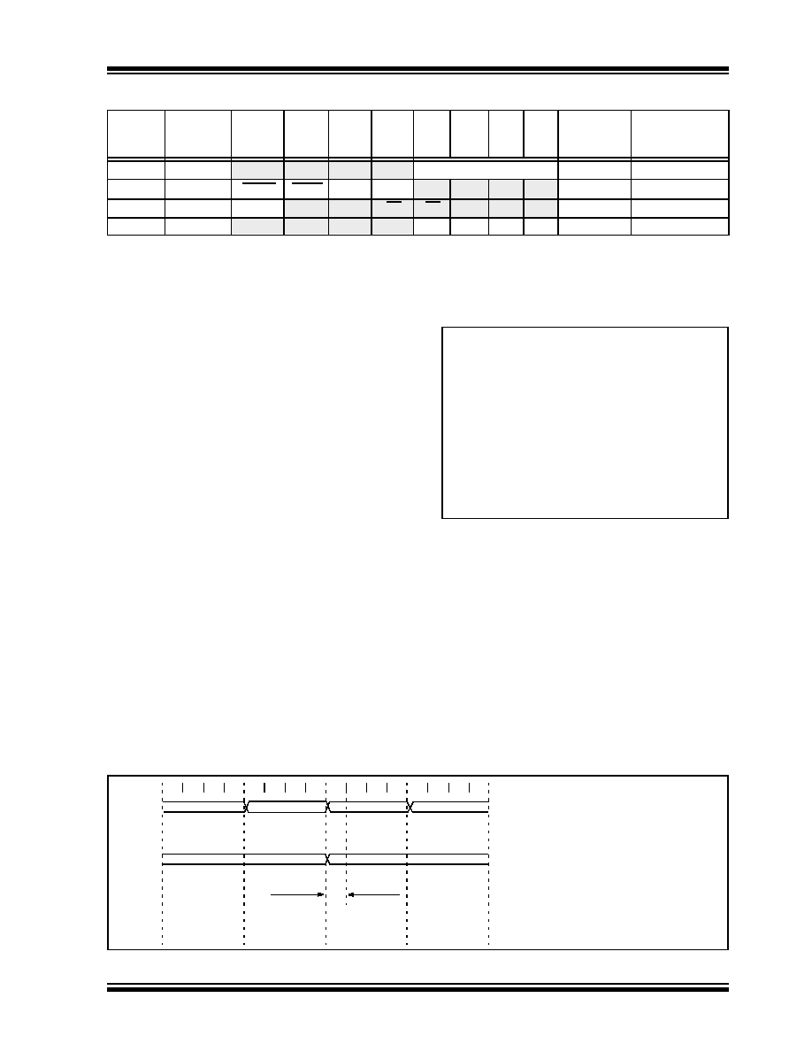
FIGURE 5-5:
SUCCESSIVE I/O OPERATION
Address
Name
Bit 7
Bit 6
Bit 5
Bit 4
Bit 3
Bit 2
Bit 1
Bit 0
Value on
Power-On
Reset
Value on
All Other Resets
N/A
TRISGPIO
—
I/O Control Registers
---- 1111
N/A
OPTION
GPWU
GPPU
T0CS
T0SE
PSA
PS2
PS1
PS0
1111 1111
03h
STATUS
GPWUF
—
TO
PD
Z
DC
C
0001 1xxx
q00q quuu
(1)
06h
GPIO
—
GP3
GP2
GP1
GP0
---- xxxx
---- uuuu
Legend:
Shaded cells not used by PORT registers, read as ‘0’, – = unimplemented, read as ‘0’, x = unknown, u = unchanged,
q
= depends on condition.
Note
1:
If Reset was due to wake-up on pin change, then bit 7 = 1. All other Resets will cause bit 7 = 0.
;Initial GPIO Settings
;GPIO<3:2> Inputs
;GPIO<1:0> Outputs
;
GPIO latch
GPIO pins
;
----------
BCF
GPIO,
1 ;---- pp01
---- pp11
BCF
GPIO,
0 ;---- pp10
---- pp11
MOVLW
007h;
TRIS
GPIO
;---- pp10
---- pp11
;
Note:
The user may have expected the pin values to
be ---- pp00. The second BCF caused GP1
to be latched as the pin value (High).
PC
PC + 1
PC + 2
PC + 3
Q1 Q2 Q3 Q4
Q1 Q2
Q3 Q4 Q1
Q2 Q3 Q4
Q1 Q2 Q3 Q4
Instruction
Fetched
GP<2:0>
MOVWF GPIO
NOP
Port pin
sampled here
NOP
MOVF GPIO
, W
Instruction
Executed
MOVWF GPIO
(Write to GPIO)
NOP
MOVF GPIO,W
This example shows a write to GPIO followed
by a read from GPIO.
Data setup time = (0.25 TCY – TPD)
where: TCY = instruction cycle
TPD = propagation delay
Therefore, at higher clock frequencies, a
write followed by a read may be problematic.
(Read GPIO)
Port pin
written here
相关PDF资料 |
PDF描述 |
|---|---|
| VE-J6P-IY-F3 | CONVERTER MOD DC/DC 13.8V 50W |
| PIC10F200T-I/MC | IC PIC MCU FLASH 256X12 8DFN |
| VE-J6N-IY-F1 | CONVERTER MOD DC/DC 18.5V 50W |
| VE-J1P-IW-F4 | CONVERTER MOD DC/DC 13.8V 100W |
| PIC10F220-I/OT | IC PIC MCU FLASH 256X12 SOT-23-6 |
相关代理商/技术参数 |
参数描述 |
|---|---|
| PIC10F220EP | 制造商:MICROCHIP 制造商全称:Microchip Technology 功能描述:6-Pin, 8-Bit Flash Microcontrollers |
| PIC10F220-I | 制造商:MICROCHIP 制造商全称:Microchip Technology 功能描述:High-Performance Microcontrollers with 8-bit A/D |
| PIC10F220I/MC | 制造商:MICROCHIP 制造商全称:Microchip Technology 功能描述:High-Performance Microcontrollers with 8-bit A/D |
| PIC10F220-I/MC | 功能描述:8位微控制器 -MCU 0.375KB 16B RAM RoHS:否 制造商:Silicon Labs 核心:8051 处理器系列:C8051F39x 数据总线宽度:8 bit 最大时钟频率:50 MHz 程序存储器大小:16 KB 数据 RAM 大小:1 KB 片上 ADC:Yes 工作电源电压:1.8 V to 3.6 V 工作温度范围:- 40 C to + 105 C 封装 / 箱体:QFN-20 安装风格:SMD/SMT |
| PIC10F220I/OT | 制造商:MICROCHIP 制造商全称:Microchip Technology 功能描述:High-Performance Microcontrollers with 8-bit A/D |
发布紧急采购,3分钟左右您将得到回复。